Hello All,
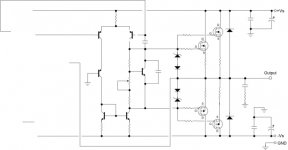
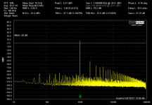
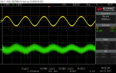
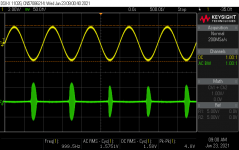
I am working on an amplifier with a topology very similar to the simasym amplifier that has been discussed at various times on this forum. The major difference is that this amplifier has a MOSFET output stage and operates at + / - 70V. This is a current commercial design, so I can not publish the complete schematic, but the attachment 1 shows the topology for the VAS and output stages. I blew it up by accidentally powering it up with out connecting the ground to the power supply. I have replaced all damaged components, and the amplifier seems to be in basic working order. The distortion spectrum (attachment 2) confirms that it is operating, but not very well. Attachment 3 shows a DSO photo with a 40 mVrms input, where the yellow trace is the output from the amplifier, and the green trace is that output after a 1 KHz passive notch filter, all looks well. However, attachment 4 shows the same setup but the input was increased to 70 mVrms. The oscillation during the bursts is about 11 MHz. The gate stopper resistors all measure within 2 ohms of the specified value. The propensity to oscillate decreases as the circuit warms up.
I would appreciate any help in directing me toward the source for those oscillation burst.
Thanks in advance for your help.
ceulrich
Attachments
I see there is a warning online about the BJT version oscillating , try increasing the value of the mosfet gate resistors otherwise changing the value of the compensation capacitor(s).
I don't know if the following is related at all or not. In the late 1980s I had an 800 watt mosfet amplifier adapted for an application by a professional audio electronic engineer. About 30 were made and used in professional systems. They did a similar thing for a few tens of seconds at switch on. The solution was two 1µF film capacitors bypassing the ±rails on the circuit board tracks at the output devices.
Last edited:
minek123, set for 100 mA cold, drifts down to around 90 mA when fully warmed up.
duncan2, the gate resistors are already at the top of the normal range, I will look into increasing the compensation capacitors.
johnmath, interesting, I will consider.
Thanks all for your interest.
Cheers,
ceulrich
@font-face {font-family:Arial; panose-1:2 11 6 4 2 2 2 2 2 4; mso-font-charset:0; mso-generic-font-family:auto; mso-font-pitch:variable; mso-font-signature:-536859905 -1073711037 9 0 511 0;}@font-face {font-family:"MS 明朝"; panose-1:0 0 0 0 0 0 0 0 0 0; mso-font-charset:128; mso-generic-font-family:roman; mso-font-format😱ther; mso-font-pitch:fixed; mso-font-signature:1 134676480 16 0 131072 0;}@font-face {font-family:"Cambria Math"; panose-1:2 4 5 3 5 4 6 3 2 4; mso-font-charset:0; mso-generic-font-family:auto; mso-font-pitch:variable; mso-font-signature:-536870145 1107305727 0 0 415 0;}p.MsoNormal, li.MsoNormal, div.MsoNormal {mso-style-unhide:no; mso-style-qformat:yes; mso-style-parent:""; margin:0in; margin-bottom:.0001pt; mso-pagination:widow-orphan; font-size:12.0pt; font-family:Arial; mso-fareast-font-family:"MS 明朝"; mso-fareast-theme-font:minor-fareast; mso-bidi-font-family:"Times New Roman"; mso-bidi-theme-font:minor-bidi;}.MsoChpDefault {mso-style-type:export-only; mso-default-props:yes; font-family:Arial; mso-ascii-font-family:Arial; mso-fareast-font-family:"MS 明朝"; mso-fareast-theme-font:minor-fareast; mso-hansi-font-family:Arial; mso-bidi-font-family:"Times New Roman"; mso-bidi-theme-font:minor-bidi;}div.WordSection1 {page:WordSection1;}
The 1µF on supply rails is my recollection, both in value and position, but it was 35 years ago. I might have some documentation on an old Microsoft PC backup somewhere; I went Apple OSX in 2005.
Are gate stoppers of the same value?
Since I don't see any RC elements around the fets, they should have the same input capacitance.
If they don't (and usually they don't) - gate stoppers should have different values.
See example below for Hitachi fets:
Let's say the 2SJ162 has a gate stopper of 100 Ohm and a gate
capacitance of 900pF, the RC time constant is just Rgate * Cgate=RC time constant, so 100 * 900x10^-12=90nS.
If we want 'balance' we need a resistance on the gate of
the 2SK1058 that gives the same time constant.
So, Rgate * 600pF = 90nS, solve for Rgate. In this case Rgate needs to be 150 Ohm.
Alternative - if input capacitances of N and P fets differ - is adding capacitor to N device.
If RC time constant of N and P fets differes too much - it ends up with oscillations.
Not sure what fets are you using, it wouldn't hurt to check their input capacitances in the sheet.
minek, thanks for that information it is really helpful. These are IR MOSFETs, and the gate stopper resistors are all the same value. I have replaced all four MOSFETs, at various times over a period of months from different DigiKey orders, could the variation in devices be my problem?
Cheers,
ceulrich
Cheers,
ceulrich
If you have some of them left, you can measure input capacitance, and see if they are consistent (N vs P).
Vertical mosfets usually are consistent... But I was only checking devices from the same batches...
Are these like IRFP240/9240 ? N/P should have almost the same input capacitance (1300pF/1200pF)
according to the specs. So they should be ok with the same gate stoppers, unless one of them is different..
I usually measure input capacitance before installing them.
But in most cases vertical fets are ok in this regard, usually they have the same gate stoppers.
Lateral fets definitely have this issue.
Last edited:
Minek, yes these are 240 / 9240 types.
I stumbled across a new problem. I checked the bias on all four MOSFETs, normally I just measure the one that is easiest to get to, and found one of the N-channel devices running >40 mV while the other three were running around 22 mV. I replaced that MOSFET with a new unit, same problem, bias running >40 mV. The other N-channel MOSFET measures 17.8 mV. I have not measured it out of circuit but the source resistor measures about right. I am stumped.
Cheers,
ceulrich
That's a big difference...
So it seems they were not matched for Vgs, you said they were from different batches...
With parallel fets you can't avoid matching... It has to be done.. Especially if they are from different batches,
but even from the same batches variance can be too big...
For me it takes at least 10 devices to select matching 4...
Last edited:
Minek, Thanks for the guidance. I have been working, off and on, for over a year on this amplifier, and I was beginning to think that matching devices might be my problem, even though I was specifically told that matching was not necessary.
This will probably turn out to be my winter project.
Cheers,
ceulrich
This will probably turn out to be my winter project.
Cheers,
ceulrich
For those following this thread, here is an update:
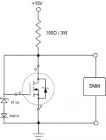
I built up an N-Channel MOSFET Test Jig per a Nelson Pass design on the passdiy.com website, and also from a thread by xrk971 on this forum.
Attachment 1 shows the schematic. At 15V the current was about 108 mA, which is close to the bias current of the amplifier.
I measured the temperature of the DUT with a surface-mount thermistor sensor bolted to the thermal pad. It took approximately 15 minutes for the temperature to equilibrate at about 40ºC. This was also similar to the operating conditions of the amplifier, where the heatsink equilibrates at about 37ºC at idle.
Using this Test Jig I measured the VGS at 3.97V for the IRFP240 removed from the board. I removed the other IRFP240 from the board, and measured the VGS at 4.00V. Both measurements were at 40ºC. If my measurements are correct, a miss-matching of VGS does not seem to be the source of the difference in bias.
The apparent runaway bias of >40 mV was taken during the first minute or two of operation, before I powered down, since I was concerned about additional damage. I will have go back and re-evaluate.
ceulrich
Attachments
Sounds more possible to be a circuit error or solder issue on the board to cause such a high mismatch in bias current.
If all of the source resistors are in spec on the N channel side.
Be a good idea to check the P channel side. Since it would affect the output rail they share.
Far as stability
The feedback network which sets the overall gain could use a small value capacitor across the resistor. usually very low around 3 pico farad
Let me add some clarification. Referring back to the schematic in post #1: Assume the left most N-channel MOSFET is Q1, and the right most is Q2. Routinely I used the source resistor for Q2 to set bias at 22mV, which resulted in Q1 running a bias of about 40-50mV, and the P-channel devices to run close to 22mV. If I use the source resistor for Q1 to set bias at 22mV, then the bias for Q2 runs at 10mV, and the P-channel devices run around 15mV.
Q1 is the MOSFET I have replaced. Q2 is the one removed, measured for VSG and reinstalled.
WhiteDragon, thanks for the suggestions.
Even though the gate stopper resistor for Q1 measured fine, I replaced it. I touched up a couple of solder joints that looked less than really shiny, but I have not (yet?) done all joints around the N-channel output stage. I have not replaced the source resistor for Q1 since it measured fine, but I am considering it. I am also considering replacing the original Q1 MOSFET, that way I will know the VGS of both N-channel devices. The bias for the P-channel devices match within about 2-6mV.
There is a 20pF capacitor across the feedback resistor.
Once I get the bias mismatch fixed, I still have the stability problem to work on. Any thoughts on why the oscillation bursts only occur during the negative phase of the signal?
ceulrich
Another update:
I touched up all the solder joints in the N-channel output stage not previously attended to. The bias difference between Q1 and Q2 was still about 10 mV. Re-installed the original MOSFET for Q1. Now the VGS for the two devices are 3.97 V for Q1 and 4.00 V for Q2. I set the bias at 22 mV using the Q2 source resistor, as has been my historical practice. After fully warming up to a heatsink temperature of around 40 – 42ºC, the bias for Q1 is 27.8 mV, and 19.5mV for Q2.
The bias difference for the P-Channel devices is 2 mV. The manufacturing codes for the N-Channel pair are the same, while the P-Channel pair have a different but matched code.
I have concluded that there was probably a flaky solder joint somewhere, but the fundamental difference in N-channel bias still exists, and is inherent to this particular selection of parts. I have a second sample of this amplifier, and it does not exhibit this bias mismatch problem.
I am back to working on fixing the oscillation bursts at the peak of the negative phase of the signal. Both samples exhibit this problem.
ceulrich
It's a very high frequency oscillation, so it seems to be mosfet related. I would probably concentrate on the P-channel side as the oscillation is triggered on the negative peaks. You could try swapping the gate diodes over to see if the problem then occurs on the positive peaks? I'd also try a bit of freezer spray on various components to see if that helps narrow it down, since you say it mainly does it from cold.
- Home
- Amplifiers
- Solid State
- Need Help with an Oscillating Amplifer