So I took a stab at what you folks have recommended but not sure I got it quite right.
From the point of view of containing the common-mode currents the extra split in the groundfill is a step backwards - now they have to go around the board between input and power supply GNDs. Best practice EMC-wise is having all ins/outs along one edge of the PCB - admittedly this doesn't produce eye-candy in terms of layout.
Ok, I'll make the changes. I see what abraxalito is saying about that slot I placed there. The other changes are easy enough. BTW, test socket on the way. I still have to get the right probe. My current one doesn't have the needed bandwidth. It falls way too short for measuring this chip. (note to self: next time, pick an op amp easier to work with)
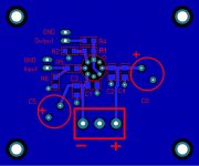
Whoops, I better clarify a point about the layouts I'm posting. I'm using an older version of Sprint Layout, and this is designed to be a 2 layer board. Green is the bottom layer and blue traces are on the top layer. There is no fill on the top layer because there is some bug that was causing it to fill in areas that were tied to the voltage rails, so would cause a short. Components will be on top side. I was planning on doing some fill manually after component layout was finalized.
This has been a great learning exercise for me! Much appreciated to everyone, even if I didn't respond or incorporate some ideas. I plan on going back through and reading all your comments more closely and some layouts that were posted as examples.
I'll update this thread as it moves along from getting boards made and verification that it is not oscillating.
I'll update this thread as it moves along from getting boards made and verification that it is not oscillating.
Last edited:
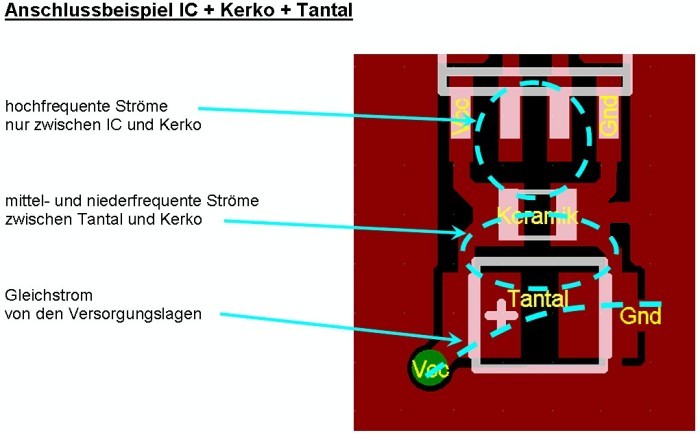
I would run power directly to the electrolytics.
Not on a wide bandwidth op amp.
Question: what is an acceptable value for the input resistor? 1k? This was brought up during initial layout but I'm not sure what value is critical to keep the stray capacitance at bay.
That should do.
no, traces from power in connector to electrolytic first then to ceramic then to amplifier.
A far as the op amp is concerned, the present arrangement is best.
- Status
- This old topic is closed. If you want to reopen this topic, contact a moderator using the "Report Post" button.
- Home
- Source & Line
- Analog Line Level
- Need an opinion on layout of LME49713 preamp