Print can be burned/damaged if the power supply has sufficient current delivery and there are no rail fuse to protect the board. Lack of rail fuses is a design choice and I've seen it many times on amplifiers.
The amp should come out of protect with a bulb tester as long as the supplies are OK (high enough) and there is no DC offset condition... which is something to check first.
Failure of outputs can take out other directly coupled stages in front of them. Sometimes it is a fault with the 'other stages' that take the outputs in the first place.
I would never risk returning the original drivers and possible the one before back to service if the amp suffered a catastrophic failure although if they are working OK then its fine to continue with bulb to make sure all is well. Then replace them would be my advice.
Just because a transistor passes a beta test @ 2 v or whatever small test voltage doesn't mean it won't short across c-e under 40 v or whatever the operating voltage is. Diodes the same way. Just because a capacitor reads the right capacitance at 2 v on a meter doesn't mean it won't short across at 40 v or whatever operating voltage is.
I said this before. Pros shotgun replace everything back one or two stages before the last place you found blown up transistors. With parts costing $8 apiece when I order them from N carolina ($8 a box) I test things either in circuit under voltage limited by the bulb box, or out of circuit with 12v series 10k series the milliammeter function of the DVM. Base open on the Vceo test for transistors.
The schematic is not on here but various people on here can spot failure voltages on collectors or capacitor ends if they do have it. In gereral on transistors in a class AB amp I expect some voltage on collector between 1/3 and 2/3 of the rail voltage (at the time limited by the bulb). Capacitors should have DC voltage between one end and the other, else why did they install it?
Sometimes one has to defeat the protection circuit to check out the amp. If it is a relay that disconnects the speaker, easy, just look at voltages before that point. Goes into of that relay should be about zero, same as DC voltage on the speaker should be 0 after protection works right.
Happy failure hunting.
Mooly and indianajo - thanks for the replies, always good information.
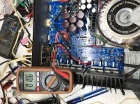
I will be replacing everything I found that was wrong (transistors, resistors and caps), then as safely as possible power it up through a 25w buld tester and looking at voltages to determine if it's safe to move up to a 40w bulb.
I will be replacing everything I found that was wrong (transistors, resistors and caps), then as safely as possible power it up through a 25w buld tester and looking at voltages to determine if it's safe to move up to a 40w bulb.
I got all the burned items replaced (including all electrolytic capacitors), transistors and a few resistors that were burned, and/or out of spec. (>10%).
Powered it up with a 25w/40w/60w bulb - no issues
Relay didn't "click" until the 60w was in place. Let it run for 15 minutes, checking temperature, DC on outputs and the "alignment proceedure".
Right channel is good - bias same right up to 18mV, very little DC on outputs (<2mV) and plays music. Only played for a few minutes and on a cheap speaker - in case the left channel went worse.
Left channel - nothing. heatsink doesn't get warm, no DC on outputs but no music either. I poked around on the replaced items (seeing if I may have had a bad solder joint) and nothing was evident.
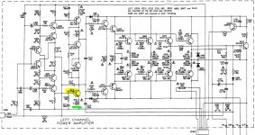
The first transistor I'm curious about is Q315 (2sc3788) - because of a lifting solder pad. The transitor may not be engaging the solder trace 100%. I plan to test further tonight. I tested the actual transistor and it tested good, but I'm just unsure the best way to work around the loose solder pads?
Helpful hints and suggestions please?! I can only think of a dremel or taking the legs directly to the next pad on the PCB - is there a better/easier method?
Best place to start testing? I get full rail voltage on the output transitor Collector (same voltage as the good channel), with Base and Emitter having mV (IIRC). Will write down tonight so I can keep the figures straight.
Added pic.
highlight the Q315 in question - Green is a resistor that was burned almost in half and caused the solder pad/trace issue. Complement of Q313.
Powered it up with a 25w/40w/60w bulb - no issues
Relay didn't "click" until the 60w was in place. Let it run for 15 minutes, checking temperature, DC on outputs and the "alignment proceedure".
Right channel is good - bias same right up to 18mV, very little DC on outputs (<2mV) and plays music. Only played for a few minutes and on a cheap speaker - in case the left channel went worse.
Left channel - nothing. heatsink doesn't get warm, no DC on outputs but no music either. I poked around on the replaced items (seeing if I may have had a bad solder joint) and nothing was evident.
The first transistor I'm curious about is Q315 (2sc3788) - because of a lifting solder pad. The transitor may not be engaging the solder trace 100%. I plan to test further tonight. I tested the actual transistor and it tested good, but I'm just unsure the best way to work around the loose solder pads?
Helpful hints and suggestions please?! I can only think of a dremel or taking the legs directly to the next pad on the PCB - is there a better/easier method?
Best place to start testing? I get full rail voltage on the output transitor Collector (same voltage as the good channel), with Base and Emitter having mV (IIRC). Will write down tonight so I can keep the figures straight.
Added pic.
highlight the Q315 in question - Green is a resistor that was burned almost in half and caused the solder pad/trace issue. Complement of Q313.
Attachments
Last edited:
I usually use solid core wire, 28 ga, wrapped around the component leg and stuck through a hole I drill in the board. Then I bend the wire over on the trace side and stick it down on the trace with solder. I have a pin vise to twirl the drill and usually use a #48 to #54 drill.
You could test your theory that the trace is not repaired by looking at the collector of Q311 (or is it 317?) to see if the DC is somewhere near the middle of the two rail voltages.
If you have an analog VOM with a 20 v AC scale or an oscilloscope, you could look at that point to see if the AC music is getting there. I put a .047 uf cap in series with the negative probe of a VOM to keep the meter from responding to DC. Use alligator clip leads.
Thanks for the replies Mooly and indianajo - very helpful.
It was the Q315 (tested as failed when I pulled it (the 2nd time)) - changed it to a KSC3503 and soldered the legs directly to the closest trace points. Used the other channel as a guide with the schematic.
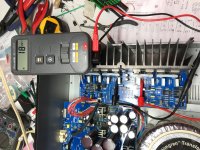
I tested with the DBT 25/40/60w bulbs without any issues. So I ran without the DBT and set the bias at 18mV. Offset on the speakers is 0mV sometimes dipping down to -1mV. Heatsinks were evenly heating, no hot/cold spots.
Let it burn-in for ~10 mins watching for any changes to bias or temperature on heatsinks. It all went well.
Plugged in my iPhone and listened to some music for 10 mins. No changes to bias or offset... so it was time to grab some actual speakers and listened for an extended time to some music (30+ mins.). No issues - sounds great!
SOUNDS GREAT!!! Thanks guys for the encouragement, suggestions and assistance getting this little beast running again.
Pics of the final product.
It was the Q315 (tested as failed when I pulled it (the 2nd time)) - changed it to a KSC3503 and soldered the legs directly to the closest trace points. Used the other channel as a guide with the schematic.
I tested with the DBT 25/40/60w bulbs without any issues. So I ran without the DBT and set the bias at 18mV. Offset on the speakers is 0mV sometimes dipping down to -1mV. Heatsinks were evenly heating, no hot/cold spots.
Let it burn-in for ~10 mins watching for any changes to bias or temperature on heatsinks. It all went well.
Plugged in my iPhone and listened to some music for 10 mins. No changes to bias or offset... so it was time to grab some actual speakers and listened for an extended time to some music (30+ mins.). No issues - sounds great!
SOUNDS GREAT!!! Thanks guys for the encouragement, suggestions and assistance getting this little beast running again.
Pics of the final product.
Attachments
 excellent. Sounds like you have a good result with this one.
- Status
- Not open for further replies.
- Home
- Amplifiers
- Solid State
- NAD 216 - Is it worth restoring/saving?