Hi,
Keypunch, I find your power ratio into active drivers of interest. Have you got this working yet?
What are your xover freq?
regards Andrew T.
Keypunch, I find your power ratio into active drivers of interest. Have you got this working yet?
What are your xover freq?
regards Andrew T.
Re: power ratio into active drivers
Hi Andrew,
lol lol lol ... sorry but I need the amps first. I am still basically running off a couple of get by with amps to power my system. Lets say I have had a life long desire for active crossover and until the internet started to bloom a few years ago, options for a DIY were far more limited on the amp/pre-amp side. I am not dealing with stereo pair which in my system. Long before Dolby 5.1 was sort of available for home use I use and still use a DSP-3000 which deals with martters beyond films/movies of the last 15 or so years. Basically what that means is I have a need for 3 stereo pairs for the DSP-3000, add dolby which adds another stereo pair, a subwoofer and centre channel which all need to be active amped excluding the subwoofer. As you can see that means 8 fullrange speakers, one two way for centre channel and one subwoofer. That means 27 amps for full three way active system or 19 amps for full 2 way active system. As you can see now the goal has not been possible until last few years from cost perspective. Even as a diy project this is still not going to be inexpensive. I have some very good pre-amps, and two basic commerical amps that are nothing to rave about. I did alot of research before the internet came alive for what crossover frequencies to use.
I created, but need to pull it off my decommissioned OS/2 system, interesting spreadsheet to combined various elements of driver size, frequency overlapping, et al formulas to come up with what crossover frequencies I could have. I cannot recall off top of my head, but the frequencies chosen were 80Hz and 3.0KHz if I recall. Part of choosing crossover points is realted to ideal, but a large part is related to driver realted parameters and affordability vs performance to ideal. I had not researched the information available now about power distribution over frequency ranges, and what types of tones exist in what frequency. That I will do later. I di dhave at time I worked out the crossover frequencies charts and such as to what frequencies different elements of music exist across as part of determining a frequency points to cross.
I choose the 100W/60W/20W as I like to have safety in headroom for dynamics. Personally if I could, I think I run on 60W/30W/10W, but again the choice of power is very much related to the crossover frequency chosen. I choose the latter large values for safety and flexibility should I need or choose to use different crossover frequencies later wihtout having to build 19-27 amps all over again 😉 .
I also have a lovely set of ribbon tweeters which will put a restriction on crossover and midrange driver selection/enclosures. These ribbon tweeters need to be crossed over at 6.0KHz minimum with a 12db slope. Ergo the midrange amp is set out to 60 to be more agile to handle the larger complex waveforms and dynamics by the amp or if I do have the LF point at 80Hz rather than 120Hz.
Remember when you are building as DIY at these 100-20W ranges the cost is not that much different. Sure higher power needs larger power supply and all which is major element of cost in DIY amp building, but power supply aside the cost of just the amp electronics is nto that much different between 60-100/30-60/30-10 for LF/MF/HF ranges.
I hope that answers your questions. If you need to discuss this more it might be good idea to open a new thread if one is not already open so this thread can keep focused on the Zeta. Just be aware I am no audio expert, and these are my current opinions based on my reseach that I will need to re-vaildate and/or update as more current information and knowledge may warrant.
Regards,
John L. Males
Willowdale, Ontario
Canada
12 December 2004 18:40
Hi lars ,
How do we decide what is the optimum power requirement of T14 as
per the wattage of the ZETA version we decide to make ,
until now you have said that it is on us if we use Irf9640 or Irfp9240 and
as per the dissipation of these devices we select the drain resistor of
T14 anywhere between 10 ohms and 47ohms .
I also want to make the 900w version of the zeta soon , but I am a little scared regarding the use of so many parallel mosfets , could anybody give a feedback if he has made the same . Lars when are YOU going to make a prototype of the PA version of the ZETA with 6 to 10 pairs of Irfp250n devices .
With regards
Rajeev
Please if anyone could post the updated schematic with all the modifications ? or email me floyds_ec@gawab.com THANX
Sivanand🙂
Sivanand🙂
A Layman's Design Inquiry
Lars,
I have three questions, but please bear with me as I am just a lay person with my own non-engineering/design mind or experience.
I assume T14, the IRFP9240 act in lieu of having to use P-Channel devices on the -Supply Rail? Is this correct? I am asking based on my humble understanding of the Zeta design.
If the answer is yest to the above question, I just ask that you humble my two questions below. A yes or no answers is all I am primarily interested in for the below two questions. If you wish to be more detailed in answers or execution of the ideas behind the two questions that is ok as well, but not expected in the questions being asked below.
The first and easiest question I have is could one use P-Channel devices instead of N-Channel devices on the -Supply Rail side if one removed T14 (IRFP0240), R29 (believe you call this a gate resistor) and the T14 Drain to -Supply Rail resistor (listed as 10 ohms in current schematic) and then connect R25 to R36? I expect the -Supply Rail output drivers will need to be oriented oppsite way or such to accomodate such a change. Again the question is basically remove T14 and T14's two associated resistors and then use P-Channel devices on -Supply Rail side instead, skipping the other details or effect the use of P-Channel output devices?
The second question is a bit harder for me to possibility atriculate in electronics/amplifier design terms, but I will do my best. Is it possible to insert a Mosfet similar to the IRFP9240 type on the +Supply side between R28 (Emitter resistor of +driver BD136) and R30 (Gate resistor of T15 first output device of +Supply Rail in such a manner and purpose that this inserted Mosfet just acts as a pass through from BD136 driver (+Supply Rail) to T15 (first output device)? In what we call assember language for computers we would call this and NOP (No Operation) instruction, which acts as placeholder in a computer without altering any state of the system. So I am basically asking if a no stage/gane change mosfet as close to the existing IRF9240 can be inserted between the BD136 driver and first output device on the +Supply Rail side of the output stage?
Lars, if I am not clear what I am asking, please do ask for clarification. Again all I ask at this point is yes/no answers, not the "details" unless you have desire to be more detailed.
Regards,
John L. Males
Willowdale, Ontario
Canada
14 December 2004 02:21
Keypunch:
1..Kind of ..
2..Yes, but then it would not fit in this thread 😀
3..It might be possible, but like the NOP has no purpose, as
there are no syncronization issues to solve. I guess the NOP was
very popular in the good ol' days of 8051 assembler..? Nowadays when everything is AVR and the brilliant Codevision C you hardly ever see a NOP anymore 🙂
Hi Lars,
Thanks for your reply (Post #406) to my Post #405. To follow up:
1) I was just curious, and provided "..Kind of.." answer is just fine for me.
2) Understand thss question would mean no longer an n-channel amp. I was asking for purpose of my own understanding.
3) This question and your answer to regarding the Zeta is where my interest is. How difficult would it be to add a mirror device to T14 to act as a NOP? The reason for this amp NOP is to balance phase on the +Rail output device(s). My assembler is much earlier than the 8051. I go back to days of vaccum tube keypunches and real iron core memory. *Wonders if makes connection to DIYAudio user name?* The primary reason for this NOP device question I have for the Zeta +Rail is to balance signal phase relationship with the -Rail that has the IRFP(240 to enable the N-Channel devices to be used on the -Rail side output devices. I grant you the IRFP9240 may represent a small difference in phase to the +rail no having a "NOP" like device, but I think it is and would be a good design to do so. I am not suggesting the design is bad. All I am saying is it seems to make sense and I assume can in fact make difference in upper and lower half wave phase relationships.
FYI, NOPs were used mostly as way to enable instructions that skip next instruction on a test condition when one reason for testing condition with a special short word branch instruction which one only wanted to set or unset a system flag. Hence no need to use these simple conditional test/branch aspect of the instruction from a logic perspective. These NOPs were popular simply because machine instruction sets were smaller in number of instructions and much smaller in amount of memory used. NOPs were also used for certain interrupt or hardware timing sensitive conditions as well.
Regards,
John L. Males
Willowdale, Ontario
Canada
15 December 2004 07:59
Hey Lars;
Hi Lars;
Can you provide me with information about the ZETA that may help me with my thinking on my own quasi-amp.
I would be grateful if you could provide the following.
1. For say rails of +/- 80 volts what is the amps maximum peak to peak voltage swing before clipping? Can you comment on this characteristic i.e can it be improved or why it can't.
2. Does this amp clip assymetrically? If not, how have has this been fixed?
Thanks for your interesting posts so far, it has progressed my learning considerably.
Cheers
quasi:
1..Something like +/- 76 V.
1,5..Yes it can be improved, but will add significantly to the complexity of the amplifier.
2..It does clip symmetrically.
🙂
1..Something like +/- 76 V.
1,5..Yes it can be improved, but will add significantly to the complexity of the amplifier.
2..It does clip symmetrically.
🙂
Hello Mik
There are several errors in your design.
You should change D/S of T14, and also C5 and C10 are not directly in parallel. There may be more errors, these were just
a couple that caught my eye. A good method is to highligt each connection in your CAD program, and then with a highlight pen, draw the same connection on the paper schematic. This way any error will be very visible.
BTW here is the new location of the ZETA page
http://www.lightball.dk/zeta.php
Mik: I am sorry but i can not give you any feedback as to wheather the PCB is ok or not, but i can see that C5 and C10 are still connected in parallel, as they should'nt be. 😉
Are you referring to the 'P' in the middle of the schematics symbol ? 😀
It was N simbol for 9240 in the shematics library but i didn't notice that until you pointed out .
Are you referring to the 'P' in the middle of the schematics symbol ? 😀
PCB Checking
Mik,
I am not sure why Lars states:
I have tried to take a look at your PCB to just see if it matches the schematic. I am no PCB expert to offer any feedback on the fine art of PCB design.
It seems you have changed a number of the part number assignments to ones used in the posted Zeta schematic. Can you post the schematic with part numbers and values that was used to design the PCB?
It takes far less time to compare your schematic to the posted Zeta schematic. It may be helpful to everyone and yourself if you use the same part numbers in your schematic as in the posted schematic where ever possible.
I do not have time to check the PCB from wiring perspective. I suspect many others will no thave time to cross reference your parts numbers to your PCB or schematic to validt e the PCB. The need to cross reference your schematic and part numbers to your PCB adds additional layers of possibility to missing or introducing errors in your PCB.
I will say the PCB you have designed looks promising and reasonability designed. You may need to find out and confirm if BD136, BD135, BC515 and/or IRFP9210 need to have own heatsinks and/or be thermally coupled to the output drivers and/or thermally coupled to some of each other. For example it may be helpful to have BD136 and BD135 placed on the PCB back to back with about 10mm space between then and enough space around them to allow a single heatsink to be used to join BD136 and BD135 so they can thermally track each other. That would mean allowing enough space for the type of PCB heatsink that has fins on both sides of heatsink and single flat piece inbetween the side fins so parts do not obstruct the heatsink. I would allow for a PCB based fin heatsink for IRFP9240 as option.
Regards,
John L. Males
Willowdale, Ontario
Canada
18 December 2004 23:52
mik said:It was N simbol for 9240 in the shematics library but i didn't notice that until you pointed out .
Is it O.K now?
Mik,
I am not sure why Lars states:
I am sorry but i can not give you any feedback as to wheather the PCB is ok or not
I have tried to take a look at your PCB to just see if it matches the schematic. I am no PCB expert to offer any feedback on the fine art of PCB design.
It seems you have changed a number of the part number assignments to ones used in the posted Zeta schematic. Can you post the schematic with part numbers and values that was used to design the PCB?
It takes far less time to compare your schematic to the posted Zeta schematic. It may be helpful to everyone and yourself if you use the same part numbers in your schematic as in the posted schematic where ever possible.
I do not have time to check the PCB from wiring perspective. I suspect many others will no thave time to cross reference your parts numbers to your PCB or schematic to validt e the PCB. The need to cross reference your schematic and part numbers to your PCB adds additional layers of possibility to missing or introducing errors in your PCB.
I will say the PCB you have designed looks promising and reasonability designed. You may need to find out and confirm if BD136, BD135, BC515 and/or IRFP9210 need to have own heatsinks and/or be thermally coupled to the output drivers and/or thermally coupled to some of each other. For example it may be helpful to have BD136 and BD135 placed on the PCB back to back with about 10mm space between then and enough space around them to allow a single heatsink to be used to join BD136 and BD135 so they can thermally track each other. That would mean allowing enough space for the type of PCB heatsink that has fins on both sides of heatsink and single flat piece inbetween the side fins so parts do not obstruct the heatsink. I would allow for a PCB based fin heatsink for IRFP9240 as option.
Regards,
John L. Males
Willowdale, Ontario
Canada
18 December 2004 23:52
Sorry guys ! I found another two mistakes in my schematics,I left out R19 and junction between T9/T10 and R15/R16 so everything I posted above is not to be used.
Since Eagle desn't have IRFP9240 in schematics library i made it myself but by mistake i put N channel mosfet simbol instead of P channel.
Lars Clausen said:
Are you referring to the 'P' in the middle of the schematics symbol ? 😀
Since Eagle desn't have IRFP9240 in schematics library i made it myself but by mistake i put N channel mosfet simbol instead of P channel.
Re: PCB Checking
Thanks Keypunch for you comments!
My pcb design corrispond to same part nubers as they are in Lars shematics except power transistors which are T15/T16/T17/T18
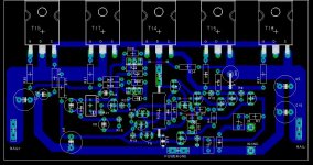
Schematics
Thanks Keypunch for you comments!
keypunch said:
It seems you have changed a number of the part number assignments to ones used in the posted Zeta schematic. Can you post the schematic with part numbers and values that was used to design the PCB?
My pcb design corrispond to same part nubers as they are in Lars shematics except power transistors which are T15/T16/T17/T18
Schematics
Attachments
Re: Re[]: PCB Checking
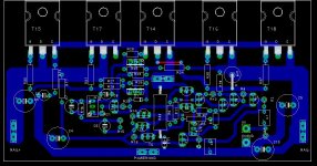
Mik,
Thnaks for posting the schematic of your design. I thought when I saw the PCB, but was not sure until the your posted schematic the output driver emitter resistors were not on the PCB. Given the output driver emitter resisters are not on your schematic, I can see why I did not see them on the PCB.
I would suggest you include the emitter resistors on the schematic and your PCB. I understadn the original schematic indicates the emitter resistors are not needed for one or two output drivers. To be honest I think it is useful to have the emitter resistors even for one pair of output drivers, but once one goes beyond one pair these emitter resistors are really important to have and use. Even if one matches the mosfets before installing on the PCB, it has already been commented from others experience once mounted and in-circuit the mosfets vary widely and have load sharing problems. Just because one has two, and has closely matched the output mosfet devices does not ensure they will "share and play nice".
I am not an engineer Mik. I just do alot of reading and see the many experiences people have had and the "expert" opinions that result before I make my own decisions what to do or what to ask. I am sure others of more knowledge will be better able to comment on the pros and cons of the emitter resistors for one output device and two output devices.
Regards,
John L. Males
Willowdale, Ontario
Canada
19 December 2004 08:45
mik said:Thanks Keypunch for you comments!
My pcb design corrispond to same part nubers as they are in Lars shematics except power transistors which are T15/T16/T17/T18
Schematics
Mik,
Thnaks for posting the schematic of your design. I thought when I saw the PCB, but was not sure until the your posted schematic the output driver emitter resistors were not on the PCB. Given the output driver emitter resisters are not on your schematic, I can see why I did not see them on the PCB.
I would suggest you include the emitter resistors on the schematic and your PCB. I understadn the original schematic indicates the emitter resistors are not needed for one or two output drivers. To be honest I think it is useful to have the emitter resistors even for one pair of output drivers, but once one goes beyond one pair these emitter resistors are really important to have and use. Even if one matches the mosfets before installing on the PCB, it has already been commented from others experience once mounted and in-circuit the mosfets vary widely and have load sharing problems. Just because one has two, and has closely matched the output mosfet devices does not ensure they will "share and play nice".
I am not an engineer Mik. I just do alot of reading and see the many experiences people have had and the "expert" opinions that result before I make my own decisions what to do or what to ask. I am sure others of more knowledge will be better able to comment on the pros and cons of the emitter resistors for one output device and two output devices.
Regards,
John L. Males
Willowdale, Ontario
Canada
19 December 2004 08:45
Re: Re: Re[]: PCB Checking
Exactly!
That's what I have been doing from the moment i found this forum.Before I wasn't so much interested for building amplifiers and audio electronics in general ,in fact electronics has nothing to do with my occupation but when I saw that someone could find information needed for this hobby that fired the spark.So, I learned how use CAD software for pcb design ,done a lot of reading about electronics and pcb design and i built my first amp, P3A four channel with mu pcb design.Of course I know that is so much to learn ,meny things which I don't understand but without people willing to help you things are little bit hard for a begginer. .😉
Cheers
keypunch said:
I am not an engineer Mik. I just do alot of reading and see the many experiences people have had and the "expert" opinions that result before I make my own decisions what to do or what to ask. I am sure others of more knowledge will be better able to comment on the pros and cons of the emitter resistors for one output device and two output devices.
Exactly!
That's what I have been doing from the moment i found this forum.Before I wasn't so much interested for building amplifiers and audio electronics in general ,in fact electronics has nothing to do with my occupation but when I saw that someone could find information needed for this hobby that fired the spark.So, I learned how use CAD software for pcb design ,done a lot of reading about electronics and pcb design and i built my first amp, P3A four channel with mu pcb design.Of course I know that is so much to learn ,meny things which I don't understand but without people willing to help you things are little bit hard for a begginer. .😉
Cheers
- Home
- Amplifiers
- Solid State
- N-Channel mosfet amplifier schematic needed