Kanwar,
how about this design,
http://www.diyaudio.com/forums/showthread.php?threadid=62620
can you simulate and highlite some points.
how about this design,
http://www.diyaudio.com/forums/showthread.php?threadid=62620
can you simulate and highlite some points.
sorry,
this is the direct link,
http://www.diyaudio.com/forums/attachment.php?s=&postid=705974&stamp=1124368531
this is the direct link,
http://www.diyaudio.com/forums/attachment.php?s=&postid=705974&stamp=1124368531

Hi!
Except for Kanwar,workhorse, amp_man1 , possibly factor etc etc all others are junk.
I am surprised you have not seen his extraordinary designs, the so claimed Nmos and MOSFET once, another one using SMPS chips and having .000 figure THD.
Come on you all still take his posts seriously.
Can this chap provide some solution to problems that he says are there. Lars posted the design after making one.
The small difference is making and NOT making.
DIY is the missing link.
Regards
Rahul
???
Rahul, I have built both of the designs I have posted thus far and both work well in different applications.
The cct in "power amp under dvelopment" whilst not a rail to rail swinger (not important really) works very well and has been scrutinized locally long and hard.
Anyway my father in law grew up in Lucknow.
Cheers
Hi!
Quasi,
I have your design on my desk top. I became interested in N Ch Mosfet due to their easy availibility and cost. Also many friends asked me for a simple ckt. I am mostly involved in RF field so looked upon others for good designs.
On the forum I have seen so many queries about the same. Till date I find only very few designs.
I began by making the MF12 by NP. It worked very well, made a few PCBs and distributed to my friends. Its posted on one of the threads.
Next in line are yours and the Zeta. Maybe later the Holton and Legendsema would also come.
R2R swing is not so important as I intend these for casual listening and for small ocassions rather than some DJ or pro audio evironment.
🙂 Nice abt your father at being Lucknow. Nice historical city very rich culture and past. Hope you may also visit one day.
BTW most of the comments were for someone else I guess you get that.
Regards
Rahul
Hi Crissty,
The design you are talking about has certain advantages as well over Zeta.
Advantages.
1. Rail to Rail output Swing ensures very high efficiency than any other design and it also earn you more dynamic headroom for free.
2. N-Vmos output stage tied directly to differential strings ensures low-cost and ultra reliable stage.
3. Very simple layout ensures DIY friendly construction.
4. Symmetric loading of driver differential ensures symmetrical slew-rate and helps in eliminating the imbalance thus avoid parasitic build up..
This design is originally from Siemens circuit book, But our Friend Quasi has done a good job towards the mentorization[tweaking] of original design and eliminated the short comings and thus making it one of the best DIYing N-Vmos design here at Diyaudio.
You can count on Quasi's reliabile designing as well, Build this design and I am sure you would not face any difficulty in setup...
me and Quasi were always here to help you.
Go for it Crissty!
regards,
K a n w a r
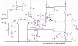
darkfenriz said:Hallo N-channelers
How about this topology?
What do you think, pros, cons ?
regards
I think this was posted earlier in a different thread (?). It is essentially JLH VAS/phase splitter/output section with a differential input stage.
I suspect the output stage works in class a as well.
I suspect you didn't look carefully or I haven't seen some similar projects, but it is intended to work in class ab.
regards
regards
Dark: do a search on the creek amp and you will see something identical to what you have.
as to what class, I guess it depends on how you set the "variable resistor" (consisting of a mosfet, a 4.7K resistor and a 4.05k pot).
to understand how the output stage works, you can combine the mosfets and their drivers into one device. the lower output device is connected to the emitter of the phase splitter (the trransistor that has a 330ohm resistor to its emitter), and the upper output device is connected to the collector of that phase splitter. so the upper and lower devices are exactly 180 degrees opposite of each other -> identical to how the jlh works.
to make it work in class ab, you will need to turn on the "variable resistor" just enough so that when the phase splitter starts to shut down, the voltage drop off the 1k and 330ohm resistors start to decrease -> turning on the upper output device.
the opposite works for the lower output device.
Hi tlf9999
Let's assume I actually understand how it should work, in fact I designed it several days ago.
In creek there is a P-ch's source driving an upper power N-ch (diamond buffer strusture) and simultanously lower N-ch by its drain. Correct me if I'm wrong, but I think it creates low open loop output Z. In contrary what I've attached is a transconductance amp ( higher output Z).
The amp I've atached isn't something completely new, there are some similar ones, for example by A. Holton. Just added some bits and pieces here and there (DC servo, inverting mode with uncommon compensation, highish current bjt drivers without output swing limitation achieved by two diodes, thermal stability) and wanted a bit of discussion and anaysis before realife amplifier synthesis. Worth?
regards
Let's assume I actually understand how it should work, in fact I designed it several days ago.
If you mean 4330 amp, than I get a bit confused.do a search on the creek amp and you will see something identical to what you have.
In creek there is a P-ch's source driving an upper power N-ch (diamond buffer strusture) and simultanously lower N-ch by its drain. Correct me if I'm wrong, but I think it creates low open loop output Z. In contrary what I've attached is a transconductance amp ( higher output Z).
In my attached amp phase splitter has a gain of 1 (330ohm both on emitter and collector) for appropiate 'work sharing' between N-CHs. In jlh it isn't vital, because it works in class A (and thus collector resistor is a pot to adjust bias). Also gain depends much on hfe of power transistors. Note that in original jlh biasing of output stage may be dependent on rail voltage, which would be a disaster in class AB.to understand how the output stage works, you can combine the mosfets and their drivers into one device. the lower output device is connected to the emitter of the phase splitter (the trransistor that has a 330ohm resistor to its emitter), and the upper output device is connected to the collector of that phase splitter. so the upper and lower devices are exactly 180 degrees opposite of each other -> identical to how the jlh works.
The amp I've atached isn't something completely new, there are some similar ones, for example by A. Holton. Just added some bits and pieces here and there (DC servo, inverting mode with uncommon compensation, highish current bjt drivers without output swing limitation achieved by two diodes, thermal stability) and wanted a bit of discussion and anaysis before realife amplifier synthesis. Worth?
regards
darkfenriz said:In creek there is a P-ch's source driving an upper power N-ch (diamond buffer strusture) and simultanously lower N-ch by its drain. Correct me if I'm wrong, but I think it creates low open loop output Z. In contrary what I've attached is a transconductance amp ( higher output Z).
But what does that P-mos do? it creates two output signals that are opposite of each other -> a phase splitter, which is precisely what the bjt does in your or jlh's design.
that's the simple point I was trying to make and I hope it comes across this time.
darkfenriz said:The amp I've atached isn't something completely new, ... Worth?
regards
and it has been tried multiple times with success. Worth it? I cannot answer that for everybody else.
hi Darkfenriz,
The circuit you have posted here suffers from cross-conduction..have you checked that? especially at 50KHZ
regards,
K a n w a r
The circuit you have posted here suffers from cross-conduction..have you checked that? especially at 50KHZ
regards,
K a n w a r
Hi Darkfenriz,
I think you have only simulated it, but dear we have prototyped a similar amp like your's 5 years ago which features same output stage and driver stage and it cross- conducts very well...
It would be very good to hear if you have prototyped it and it is not cross-conducting!
regards,
K a n w a r
I think you have only simulated it, but dear we have prototyped a similar amp like your's 5 years ago which features same output stage and driver stage and it cross- conducts very well...
It would be very good to hear if you have prototyped it and it is not cross-conducting!
regards,
K a n w a r
Hello All ,
I had made the Zeta with two pairs of output devices , due to reasons unknown to me one output device from each side failed , I disconnected them and the amp started working OK , now it is many months and the amp is working very fine , I have installed the amp in a monitor cab and have used the same in many programmes without any problems sometimes it is on throught the day . Hence now I can say that I have time tested the Zeta in the field and it is a very good design .
I had made the Zeta with two pairs of output devices , due to reasons unknown to me one output device from each side failed , I disconnected them and the amp started working OK , now it is many months and the amp is working very fine , I have installed the amp in a monitor cab and have used the same in many programmes without any problems sometimes it is on throught the day . Hence now I can say that I have time tested the Zeta in the field and it is a very good design .
- Home
- Amplifiers
- Solid State
- N-Channel mosfet amplifier schematic needed