What is misplaced is simply the use of the term current feedback. It already had a meaning, and a quite different one. They should have come up with some new name for it, instead of abusing existing terminology.
Of course the claim that it "started to gain exposure some three decades ago" in 2017 is complete nonsense. Valve amplifiers with shunt feedback at the output, series feedback to the cathode of the input valve have been around for much longer than that, and have been produced by the millions. It probably illustrates Sergio Franco's lack of historical awareness that also causes him not to recognize abuse of terminology.
In any case, we had this discussion before, we will never agree on it and it's only a semantic discussion anyway.
Last edited:

You have confused current controlled output with current feedback. Current feedback, if that was ever used to describe an amplifier with current as the controlled output quantity, would have just been plain wrong. I worked designing industrial instrumentation for 7 years (and marketing it for 8 years) and never ever used the term 'current feedback' to describe a 4-20mA instrumentation loop that usually used voltage feedback to set the output current. if not called a4-20 mA lop, it was just called a 'current output amplifier'. It's highly unlikely Prof Sergio Franco, a well-known figure in semiconductor circles, is unaware of any historical context wrt this subject and its relationship to tube circuits or otherwise.
Current feedback (the way the feedback signal is fed back to the error amplifier) and current controlled output (the controlled output quantity) are two very different things. I, and many others, tried to explain this to Michael Kiwanuka and a few others on this forum but to no avail.
Your confusion does not constitute a semantic problem on my part or anyone else. The two terms as I have described them are distinct and different. Read the Sergio Franco articles please.
https://engineering.sfsu.edu/welcome-sergio-franco-home-webpage
Could you please read the section containing Fig. 3 in https://linearaudio.net/sites/linearaudio.net/files/Farren feedback1938.pdf ?
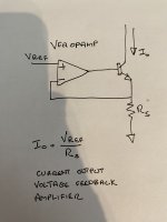
That is a current output amplifier with voltage feedback Marcel. You can see that because the input ports on the left-hand side of the black box amplifier are designated e1 and the ground to signal input e. Unfortunately, the author used the wrong term to describe his circuit, despite his very detailed and thorough math and analysis. The circuit in Figure 3 is exactly how I would depict a 4-20mA instrumentation loop amplifier if I was explaining it to someone. By comparing the voltage sensed across the resistor to a reference voltage, you get a controlled current output, so for Fig. 3, assuming infinite open loop gain, e = e1 = I.Rc so e1/Rc = I. The left-hand side of the Rc is the feedback voltage.
Sergio Franco's article shows that it is the feedback current that controls the voltage output of a voltage output CFA. The math and a very good intuitive explanation for why this is so is detailed in the link I posted. If you recall, there was a protracted discussion on this subject here over many months which was eventually shut down. I did not know it at the time, but some of the protagonists took their battle to the pages of EDN which then prompted Franco's intervention and some further interaction with people from the semiconductor applications area weighing in with Franco.

Sergio Franco's article shows that it is the feedback current that controls the voltage output of a voltage output CFA. The math and a very good intuitive explanation for why this is so is detailed in the link I posted. If you recall, there was a protracted discussion on this subject here over many months which was eventually shut down. I did not know it at the time, but some of the protagonists took their battle to the pages of EDN which then prompted Franco's intervention and some further interaction with people from the semiconductor applications area weighing in with Franco.
Attachments
I agree with Marcel. In the context of "current feedback," the term "current" refers to the variable being sensed by the feedback, such as velocity feedback or temperature feedback. In contrast, in Franco's interpretation, "current" denotes "the predominant nature of the signal fed back to the summing node," and suggests inherently fast operation. It's important to note that a low input impedance of the summing point does not necessarily result in fast operation.
I disagree Dimitri. Unfortunately the author of the original paper never thought through his nomenclature IMV and this has led to a lot of misinterpretation over the years. Thousands of semi-conductor design professionals including Scott Wurcer RIP, Walt Jung et al, academics of which Francisco and Middlebrook are just two, understand the clear distinction between feedback current and current output.
Attached from the above linked tutorial page is the often used Voltage-Series graphic along with its explanation
stating that the the series connection with the input is evident. To me it's not.
The two terminal output of the beta block should be though of as floating, for example as if it were transformer coupled.
Then those two terminals can be connected in any manner you wish. In that attached voltage series feedback diagram,
the input loop is broken and the two floating beta output terminals are inserted, in series with the input loop.
That is a current output amplifier with voltage feedback Marcel. (...) Unfortunately, the author used the wrong term to describe his circuit, despite his very detailed and thorough math and analysis.
Can you show me an article older than 1938 that uses the term the way you and your professor do?
If so, I will immediately choose your side.
If not, I can only conclude that current feedback used to be defined as Farren used the term in 1938, and that it was later redefined. (Redefined twice, in fact, as professor Nordholt uses it in yet another sense: shunt feedback at the input, series at the output.)
In either case, the discussion is semantic.
I think Farren was the first, but it does not mean we cannot correct or refine his nomenclature, and especially when it has created such confusion and in the light of subsequent developments ie in this case, the invention of the CFA. In a CFA, it is the current flowing into the low Z summing node minus that flowing out via the gain setting resistor which flows into the trans admittance second stage that determines the loop gain. If that’s how it works, what other name do you want to give it other than current feedback? If I look at Farren’s Fig. 3, it’s clear the feedback signal is a voltage signal and his math over the page says exactly that as well 😊
I would call it a feedback amplifier with a low open-loop input impedance at its negative input, but I guess someone from marketing could come up with a more catchy phrase.
As an aside, the engineers working on the first Philips CD players with single-bit converters wanted to call it a CD player with single-bit converters, but marketing didn't like it - why would anyone buy a Philips 1 bit CD player when they could get an 18 bit CD player from the competition? Hence, the marketing team came up with the name bitstream.
As an aside, the engineers working on the first Philips CD players with single-bit converters wanted to call it a CD player with single-bit converters, but marketing didn't like it - why would anyone buy a Philips 1 bit CD player when they could get an 18 bit CD player from the competition? Hence, the marketing team came up with the name bitstream.
Maybe this is a good time to ask about one of the things that I can't seem to get right .
Attached from the above linked tutorial page is the often used Voltage-Series graphic along with its explanation stating that the the series connection with the input is evident. To me it's not.
I'm not sure if this will help or just worsen the confusion, but let's try.
Schematic A is a copy of what you have shown.
Schematic B is an implementation with ideal components. The forward path has been replaced with a nullator (network element that has zero voltage across it and zero current through it, usually used as an ideal model for an input stage of a feedback amplifier) and a norator (network element that can conduct any current and have any voltage across it, usually used as an ideal model for an output stage of a feedback amplifier). The feedback has been implemented with a voltage-controlled voltage source with voltage gain beta. It is clear that the signal source, controlled voltage source and nullator are all in series, while the load, sense points for the controlled source and norator are all in parallel. Hence, series feedback at the input, parallel or shunt feedback at the output.
Schematic C is the same with an extra wire between the input and output side. In this schematic, the extra wire doesn't do any harm, as it conducts no current.
With the extra wire in place, the controlled source can just as well be replaced with a voltage divider, this leads to schematic D.
An attempt to replace the nullator and norator with something more practical leads to schematic E. It is a signal schematic, everything that is required for biasing is left out.
Last edited:
All in all, I think it gets messy when you replace the ideal parts with more practical circuits. How to connect a controlled source in series with something or its controlling terminals in parallel with something is clear, but what does series or parallel even mean for a voltage divider with its three terminals? The answer becomes clear (to me anyway) when you see the voltage divider as a practical implementation of a voltage-controlled voltage source with a gain beta < 1.
Fair enough. So we could abbreviate it LOLII-ANI 😊I would call it a feedback amplifier with a low open-loop input impedance at its negative input, but I guess someone from marketing could come up with a more catchy phrase.
As an aside, the engineers working on the first Philips CD players with single-bit converters wanted to call it a CD player with single-bit converters, but marketing didn't like it - why would anyone buy a Philips 1 bit CD player when they could get an 18 bit CD player from the competition? Hence, the marketing team came up with the name bitstream.
I think in this case we unfortunately have to give credit to the marketing team here.why would anyone buy a Philips 1 bit CD player when they could get an 18 bit CD player from the competition?
Because the majority of buyers doesn't understand a thing about all the technical aspect and just thinks more = more better.
But these cases are rare.
I have seen "24 bit" ADC's that barely reach 18 bits of performance.
I will attempt to explain in non-mathematical terms feedback applied to a differential input amplifier. Without feedback a differential amplifier is made to have a very very high gain. The voltages at the differential amplifier follow each other closely and are in fact almost equal with a small error difference. One voltage at the differential input is intentionally made to be equal to a fraction of the output, say 1/40, although other fractions are used. This means, the input signal has to follow very closely 1/40 of the output voltage. The very small insignificant difference between the voltages at the input is what drives the output and is governed by the open loop gain. This very small voltage can be seen as the distortion voltage and is very small compared to the output at all output voltages.
Rayma, Marcel. Thank you . These are the descriptions I needed in order to make some sense of the block diagrams.
There's enough posted above to keep a body busy for a good while. Somewhere between 10 and 50 readings should have it all feeling like it's something I've known since I was 2. There are terms there I've seen before but never known anything about so this is a great opportunity. Thanks !
In the meantime, I'm trying to sort out a circuit I have on the bench and to get deeper understanding of the feedback network in the circuit posted in #530 , any answers you can give would help on both fronts (ie. understanding his circuit and understanding the terminology that others use for feedback. )
Tritschler calls the 2nd stage feedback network of his RIAA circuit (attached in post #530 ) "Shunt-Shunt" so shunt derived, shunt applied , which simplified would look like this.

It's easy enough to see that the feedback network is a simple resistive divider in parallel with the triode and shunting signal around it while allowing a portion of the signal to be fed back into the input. But why the dual hyphenated designation Shunt (derived) - Shunt (applied) and not just simply parallel?
To understand this better, the questions below:
What changes if it becomes Series - Shunt ?
What changes if it becomes Shunt - Series ?
What changes if it becomes Series - Series ?
BTW, I'm not ignoring Bonsai's explanation in post #527, just asking the question this way for view from a different angle.
Thanks !
Yes, I get it now. That removes my insistence on trying to make them equivalent. Thanks .so you see that you cannot directly translate the triangle pins to triode pins.
There's enough posted above to keep a body busy for a good while. Somewhere between 10 and 50 readings should have it all feeling like it's something I've known since I was 2. There are terms there I've seen before but never known anything about so this is a great opportunity. Thanks !
In the meantime, I'm trying to sort out a circuit I have on the bench and to get deeper understanding of the feedback network in the circuit posted in #530 , any answers you can give would help on both fronts (ie. understanding his circuit and understanding the terminology that others use for feedback. )
Tritschler calls the 2nd stage feedback network of his RIAA circuit (attached in post #530 ) "Shunt-Shunt" so shunt derived, shunt applied , which simplified would look like this.
It's easy enough to see that the feedback network is a simple resistive divider in parallel with the triode and shunting signal around it while allowing a portion of the signal to be fed back into the input. But why the dual hyphenated designation Shunt (derived) - Shunt (applied) and not just simply parallel?
To understand this better, the questions below:
What changes if it becomes Series - Shunt ?
What changes if it becomes Shunt - Series ?
What changes if it becomes Series - Series ?
BTW, I'm not ignoring Bonsai's explanation in post #527, just asking the question this way for view from a different angle.
Thanks !
R6 and C3 are the shunt-shunt feedback network. They approximate a voltage-controlled current source with frequency-dependent transfer. (When you try to make a shunt-shunt feedback with some other type of controlled source, you end up shorting the signal - I have to come back to that later.) Due to the voltage to current conversion in the feedback, the whole stage is a current to voltage converter.
R4, C1 and R5 are a π filter between the first and the second stages.
V2 is the implementation of the nullator and norator. A single triode can do the job because the nullator and norator happen to have a common node, they are both connected with one side to (AC) ground. A triode also has such a common terminal, as its cathode is both an input and an output.
C2, R7, D2, C4, R9 and R8 are for biasing.
Four attempts to make an amplifier with parallel feedback at the input and output using a nullator, a norator and a controlled source.
A and B can't work because they short the output.
C doesn't directly short the output, but as the voltage across the nullator is zero by definition, so is the controlled voltage source's output voltage. Assuming a linear controlled source, the same holds for its input voltage, which is also the output voltage of the amplifier. That is, C doesn't work either.
D works just fine. The output voltage is adjusted such that the current is flows into the voltage-controlled current source, which means that the transfer from is to the output voltage is the reciprocal of the transfer of the controlled source.
Last edited:
Alright, you've given me a year's worth of study. Seriously ! Reading definitions of Nullors shows me I'm seriously out of my depth as far as understanding the practicable side of these concepts. Nevertheless . . . . .
So , to understand the voltage controlled current source designation could I say that any circuit over which a change in voltage results in change of current fits that name?R6 and C3 are the shunt-shunt feedback network. They approximate a voltage-controlled current source with frequency-dependent transfer.
One question about that specific feedback circuit. It is billed as bass boost , but from what I can tell it actually attenuates the higher frequencies, not boost the lower ones. Am I missing something?They approximate a voltage-controlled current source with frequency-dependent transfer.
Marcel, do I need to ship some paper to you? 😉View attachment 1333155
Four attempts to make an amplifier with parallel feedback at the input and output using a nullator, a norator and a controlled source.
A and B can't work because they short the output.
C doesn't directly short the output, but as the voltage across the nullator is zero by definition, so is the controlled voltage source's output voltage. Assuming a linear controlled source, the same holds for its input voltage, which is also the output voltage of the amplifier. That is, C doesn't work either.
D works just fine. The output voltage is adjusted such that the current is flows into the voltage-controlled current source, which means that the transfer from is to the output voltage is the reciprocal of the transfer of the controlled source.
- Home
- Design & Build
- Electronic Design
- Myths, tricks and hey, that's neat!