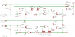
is the attached schematic with DN2540 CCS correct?
Yup, it looks OK.
BTW, I was simulating a 2-BJT + 3 resistor + 1 bootstrap cap CCS that simulates better than all of the three (regulator, resistor and JFET) topologies I posted earlier in post #297. The advantage is that it works fine with commodity BJTs (BD139/140, BC54x/BC55x). The challenge is in finding space for it.
Yup, it looks OK.
Thanks Siva 🙂
The advantage is that it works fine with commodity BJTs (BD139/140, BC54x/BC55x). The challenge is in finding space for it.
Yet to be refined but for the depletion mosfets I've found a possible solution (see attachment).
Can you post the schematic of your CCS so I can try to fit it on board?
It would be fantastic if you manage to simulate also the cascoded depletion mosfet CCS.
Attachments
Last edited:
Can you post the schematic of your CCS so I can try to fit it on board?
It would be fantastic if you manage to simulate also the cascoded depletion mosfet CCS.
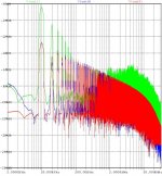
OK - here are some quick and dirty simulations of my BJT CCS (OUT4) and your cascoded MOS CCS (OUT5) - source resistor adjusted to 62 ohms to normalize the CCS current to approx. 20 mA for both. Surprising result! They perform nearly identically, and better than the LT1086 regulator. They're also better than the single JFET and plain resistor, but I've omitted those FFT curves.
Attachments

Last edited:
I would suggest that you simulate drain as the load. Just like simulation of MyRef damping.OK - here are some quick and dirty simulations of my BJT CCS (OUT4) and your cascoded MOS CCS (OUT5) - source resistor adjusted to 62 ohms to normalize the CCS current to approx. 20 mA for both. Surprising result! They perform nearly identically, and better than the LT1086 regulator. They're also better than the single JFET and plain resistor, but I've omitted those FFT curves.
I would suggest that you simulate drain as the load. Just like simulation of MyRef damping.
I don't understand. I have a 1k resistive load which draws ~12mA, comparable to the max. current of the LM318. Could you explain "drain as load"?
Surprising result! They perform nearly identically, and better than the LT1086 regulator.
Thanks Siva 🙂
Help me to understand, those FFT curves represent rejection, right?
Can you also simulate output impedance?
Can you estimate power on DN2540? It would be nice if TO-92 is suitable for both upper and lower transistor.
Last edited:
... your cascoded MOS CCS ...
Sorry, that should read "Unixman's/your cascoded MOS CCS ..." - the edit window expired.
BTW, without the bootstrap, the BJT CCS performs worse than the cascoded MOS.
I don't understand. I have a 1k resistive load which draws ~12mA, comparable to the max. current of the LM318. Could you explain "drain as load"?
If you only provide constant current drain, it is different from dynamically varying of drain in actual use.
Like in damping simulation, the left hand side would be a constant voltage source instead of your AC, at the drain, it would be more realistic to apply AC current source in series with a resistor. Then you will simulate how load effects the voltage.
Help me to understand, those FFT curves represent rejection, right?
Can you also simulate output impedance?
Yup, the FFT curves represent rejection of a 1V amplitude sinusoidal signal added to the 32V DC input. (To be accurate, I should have normalized it to 1V rms ~ 1.4142V amplitude, so the dB numbers could directly be interpreted as PSRR values, but it's only about 3dB off. It's fine for comparisons.)
Output impedance can be separately simulated, but you can approximately obtain it by inspection. For the CCS + plain zener, it's just the incremental (dynamic) impedance of the zener. For the CCS + zener + BJT beta multiplier, it's the incremental impedance of the zener divided by current gain of the BJT. In both cases, the CCS has an impedance of ~infinity and doesn't enter the picture.
are you calling C2 a "bootstrap"?without the bootstrap, the BJT CCS performs worse than the cascoded MOS.
All it is doing is trying to hold a more constant voltage across the CCS, so that it is less influenced by voltage changes between load and supply. I don't recall hearing anyone else calling that a bootstrap.
It is no different to a capacitor from supply to ground to aid more constant voltage to a load. We call that decoupling, or smoothing, but not a "bootstrap".
Like in damping simulation, the left hand side would be a constant voltage source instead of your AC, at the drain, it would be more realistic to apply AC current source in series with a resistor. Then you will simulate how load effects the voltage.
This can be easily be obtained from an output-Z calculation for the shunt regulator. The CCS has an ideal impedance close to infinity and will drop out of picture, leaving only the shunt section providing the source-Z. For the zener + BJT beta-multiplier, it will be a few 10s of ohms / beta - typically less than 1 ohm dynamic impedance, maybe as low as 0.1 ohms.
Can you estimate power on DN2540? It would be nice if TO-92 is suitable for both upper and lower transistor.
Quick and dirty: 20 mA * (32 - 12 - 20mA*62 ohms) = 20 mA * (20 - 1.24) ~= 0.4W, split across both the DN2540s at 20 mA. However, most of the voltage drop is across the upper DN2540, and hence also the power dissipation. I'd estimate something like 0.36W + 40 mW. It's barely OK with TO-92s, but the upper one will get a bit toasty, even at 20 mA bias. If you go with a higher CCS current, the upper DN2540 will have to be a TO220.
are you calling C2 a "bootstrap"?
All it is doing is trying to hold a more constant voltage across the CCS, so that it is less influenced by voltage changes between load and supply. I don't recall hearing anyone else calling that a bootstrap.
It is no different to a capacitor from supply to ground to aid more constant voltage to a load. We call that decoupling, or smoothing, but not a "bootstrap".
Well, it tries to keep the current through R4 (and hence the BJT currents) constant, regardless of dips/spikes at the source. IMHO, this would be a bootstrap - similar to bootstrapped VAS topologies. Whatever it is called, it is essential to the performance of the BJT CCS. If the R-C-R section is replaced by a single R, performance is significantly degraded.
I think the trend of the curve over the audio spectrum is more important than the simple calculation.This can be easily be obtained from an output-Z calculation for the shunt regulator. The CCS has an ideal impedance close to infinity and will drop out of picture, leaving only the shunt section providing the source-Z. For the zener + BJT beta-multiplier, it will be a few 10s of ohms / beta - typically less than 1 ohm dynamic impedance, maybe as low as 0.1 ohms.
In both cases, the CCS has an impedance of ~infinity and doesn't enter the picture.
Thanks 🙂
So the important part is the rejection.
The CCS has an ideal impedance close to infinity and will drop out of picture, leaving only the shunt section providing the source-Z. For the zener + BJT beta-multiplier, it will be a few 10s of ohms / beta - typically less than 1 ohm dynamic impedance, maybe as low as 0.1 ohms.
Very interesting.
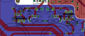
ClaveFremen and LinuxGuru: What are the actual sizes of your PC boards?
FE bords are 114.3 x 100.33 mm
Just tried the LM317 CCS also for the -14V regulator and it seems to sound slightly better than the LM337 one.
Not a day and night difference though.
Now I'm going to put on breadboard the depletion mosfet CCSs.
Not a day and night difference though.
Now I'm going to put on breadboard the depletion mosfet CCSs.
FE bords are 114.3 x 100.33 mm
And that's the My_Ref_FE - PCB from your Google Docs library?
LinuxGuru, what are the dimensions on your v1.4 PCBoard, please? 🙂
- Status
- Not open for further replies.
- Home
- Amplifiers
- Chip Amps
- My_Ref Fremen Edition - need help on PCB evaluation