level shifter
Hi IVX,
<I'm still so stupid.. please attach IMG for explanation.>
You do very well compared to me, in IMHO, anyway.
I hope this diagram helps. I have not ever tried it in actual circuits but considered it for switching power supplies in the past. However, it does not work for them. But it may work for class D since the output mosfets do not have to stay in high impedance mode. In our class D methods so far, the output is either high or low.
R1 must dissipate power from the full voltage of the amplifier PS until M3 turns off. But this time should be very short compared to the of the peiod of the output waveform.
Attachments
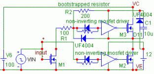
The ratio R2/R1 may need to be at least 7/1 instead of 2/1. So maybe R2=1500 and R1=200 would be better. But if R2 is too large, the mosfet driver gate may try to switch low again as the mosfet driver is pulled high by M3. also, M1 needs to conduct pulses greater than its long term current rating. Gate resistors should be used for M1,M2, and M3. 
Hi subwo,
I tried this circuit already in 1999 - it's not worked properly, be cause when M1 is turn
on M3 is turn off and entire upper driver flying down together with drain of M1. More
stability gives opposition working by inverting mosfet driver.This approach not so fast
that can be replaced to IR chip yet.
Best regards.
Hi IVX,
I understand. I think speed is not needed for a sub amp anyway. So, the IR2113 is good for powerful sub amps. But maybe for the rest of the audio spectrum, something with one P-channel and one N-channel output is fine.
Best Regards.
I understand. I think speed is not needed for a sub amp anyway. So, the IR2113 is good for powerful sub amps. But maybe for the rest of the audio spectrum, something with one P-channel and one N-channel output is fine.
Best Regards.
Oh no..anything only no P.
Actually, 4 pulse transformers (1-turn on hi drv, 2-turn off hi drv, 3-turn on low drv, 4-turn off low drv) 2 flip-flops and 2 MAX5048 -will be fastest.No any voltshifters..
2113 for sub can gives best around performance.
Actually, 4 pulse transformers (1-turn on hi drv, 2-turn off hi drv, 3-turn on low drv, 4-turn off low drv) 2 flip-flops and 2 MAX5048 -will be fastest.No any voltshifters..
2113 for sub can gives best around performance.
<I was thinking the same thing about pulse transformers.> = I was working the same work about repair business.
It is interesting to construct a subwoofer amp without radiators in general, by using minimal Fsw (~20khz) and many D2pack mosfets.. it's seems as a miracle!..in fact for 50w less for 2xirf540n (50khz) radiator not needed
It is interesting to construct a subwoofer amp without radiators in general, by using minimal Fsw (~20khz) and many D2pack mosfets.. it's seems as a miracle!..in fact for 50w less for 2xirf540n (50khz) radiator not needed
Hi all,
After thinking about PS pumping problem
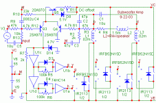
caused by even a small DC offset or low frequency reproduction, I have determined that my last class D sub amp circuit posted a few pages earlier in this thread can easily be converted to full bridge to eliminate those problems while also allowing a 4X increase in power output.
The new circuit can be done easily by stacking one IR2113 on top of the other. This way, the circuit paths are very short making the size small and EMI less. The pins not sharing the exact same circuitry like the bootstrapped power supplies and the input and output pins can be bent outward. Then the components can be soldered directly onto those pins. The entire amp, not counting the heatsinks, output chokes, and filter capacitor should take up an area of no more than 9 square inches. I think the amp should be able to put out 1000Wrms if the mosfets are cooled with a fan, the power supplies are +/-60V at 1KW, and the mosfets are mounted on a 3X3 inch microprocessor heatsink. The link at the bottom gives ideas for building high power switchmode power supplies.
The simulations indicated the current mirror to be a source of considerable distortion. Therefore, it is omitted from this version. The current source is now changed to constant current to regulate the DC offset. It may be possible to control the DC offset even tighter by deriving the voltage for the mosfet driver control circuitry from a regulator transistor. That transistor's base would be controlled by the the voltage created by the current from the feedback transistor passing through a resistor whose value is about twice that of the resistor on the signal input gate of the control circuit. Also the base of that transistor would be shunted with a filter capacitor. By the way, the Zener diode protecting the signal input gate of the control circuitry should be a 1N4148 diode turned around and connected to the control power supply positive instead of the common.
As with the older design, the oscillation frequency can be lowered by increasing the output filter choke values or the output filter capacitor. The oscillation frequency can also be lowered by increasing the value of the base resistors, R1 and R2 of the differential BJT pair. The frequency can be increased by decreasing the values of those same components. The frequency should idle at 100khz and drop down to around 25khz at peak output. This variation of frequency raises the efficiency a lot because the mosfets have to switch less at full power. But the decrease in frequency does not increase the ripple much at the output.
I would like to be able to build the circuit to test it out. But, in case I don't get the chance, I am sharing the design beforehand even though I cannot say if the circuit works in real life. At the least it would need some adjustments.
Best wishes.
After thinking about PS pumping problem
caused by even a small DC offset or low frequency reproduction, I have determined that my last class D sub amp circuit posted a few pages earlier in this thread can easily be converted to full bridge to eliminate those problems while also allowing a 4X increase in power output.
The new circuit can be done easily by stacking one IR2113 on top of the other. This way, the circuit paths are very short making the size small and EMI less. The pins not sharing the exact same circuitry like the bootstrapped power supplies and the input and output pins can be bent outward. Then the components can be soldered directly onto those pins. The entire amp, not counting the heatsinks, output chokes, and filter capacitor should take up an area of no more than 9 square inches. I think the amp should be able to put out 1000Wrms if the mosfets are cooled with a fan, the power supplies are +/-60V at 1KW, and the mosfets are mounted on a 3X3 inch microprocessor heatsink. The link at the bottom gives ideas for building high power switchmode power supplies.
The simulations indicated the current mirror to be a source of considerable distortion. Therefore, it is omitted from this version. The current source is now changed to constant current to regulate the DC offset. It may be possible to control the DC offset even tighter by deriving the voltage for the mosfet driver control circuitry from a regulator transistor. That transistor's base would be controlled by the the voltage created by the current from the feedback transistor passing through a resistor whose value is about twice that of the resistor on the signal input gate of the control circuit. Also the base of that transistor would be shunted with a filter capacitor. By the way, the Zener diode protecting the signal input gate of the control circuitry should be a 1N4148 diode turned around and connected to the control power supply positive instead of the common.
As with the older design, the oscillation frequency can be lowered by increasing the output filter choke values or the output filter capacitor. The oscillation frequency can also be lowered by increasing the value of the base resistors, R1 and R2 of the differential BJT pair. The frequency can be increased by decreasing the values of those same components. The frequency should idle at 100khz and drop down to around 25khz at peak output. This variation of frequency raises the efficiency a lot because the mosfets have to switch less at full power. But the decrease in frequency does not increase the ripple much at the output.
I would like to be able to build the circuit to test it out. But, in case I don't get the chance, I am sharing the design beforehand even though I cannot say if the circuit works in real life. At the least it would need some adjustments.
Best wishes.
Attachments
IVX said:Hi all
United States Patent 6,385,056 anybody saw it?
regards.
Hi IVX,
My computer does not have a fully functional browser. I cannot see the diagrams. Could you explain the patent and what is good about it?
Best wishes.
subwo, sorry, but i have some critical notes about your circuit again.. In the reality we not have identity of the all parts after the U1a&U1b..it will be much worse THD then 2 half bridge amp connected as H bridge.
Thanks IVX. 🙂 I would not have noticed it if you had not mentioned it. I think I can work on giving it a balanced input if needed. But why won't both halves act the same? Will not the feedback action on one side be copied for the other side?
The parts after U1 are two IR2113 driving four IRFB52N15D. I have decided it is easy to stack one IR2113 on top of the other.
The parts after U1 are two IR2113 driving four IRFB52N15D. I have decided it is easy to stack one IR2113 on top of the other.
IVX said:Hi subwo
u must download plugin..see help!
regards.
I looked at the diagrams. The last one is key. Actually, the actual I^2PS control circuitry is most likely relatively complex.
oh yes, the patent this difficult for understanding that i cannot find any advantages of it.
<The parts after U1 are two IR2113 driving four IRFB52N15D> and 2 coils
<Will not the feedback action on one side be copied for the other side?> ok - so will if use full copies of these parts.. you have it?
I don't say how much exactly, but THD will be worse of course.
<The parts after U1 are two IR2113 driving four IRFB52N15D> and 2 coils
<Will not the feedback action on one side be copied for the other side?> ok - so will if use full copies of these parts.. you have it?
I don't say how much exactly, but THD will be worse of course.
<ok - so will if use full copies of these parts.. you have it?>
Yes, exact copies. I think the distortion may be a little more too, but then with the elimination of PS pumping which also worsens distortion, the net benefit may be less distortion.
<oh yes, the patent this difficult for understanding that i cannot find any advantages of it.>I am not a big fan of these complicated methods for just a little benefit. Before I knew anyone else had discovered syncronous rectification, I put some effort into making it practical. But the timing and such things is just so critical, It is not usually worth the effort.
To use one feedback network for the full bridge there is enough, whether or not?
Hi subwo,
Subwo, I think that for you and for me desirable to hear opinion of skilled members such as Charles and Jaka Racman?
Best regards.
Hi subwo,
Subwo, I think that for you and for me desirable to hear opinion of skilled members such as Charles and Jaka Racman?
Best regards.
Hi Subwo
Since you
1.) .... take feedback exclusively from the filter output and
2.) ... already have a differential input stage....
... I would take feedback from both outputs by the use of the differential amplifier if I were you.
The two halves of your H-bridge will never be exactly the same so it is better to take the properties of both into consideration by taking NFB from both.
Regards
Charles
- Status
- Not open for further replies.
- Home
- Amplifiers
- Class D
- My very first Class D pwm (switching) amplifier.