I can't help with distortion, but power prediction is easy.jerluwoo said:So anyone out there that has some proper test equipment out there care to throw one of these together and post some numbers for us? Distortion, power out etc.. I've always been really interested to find out these things since I first built the circuit. I can sim all that but it isnt the same.
Take your Iq value and your minimum load value (R).
P=2 * I^2 * R
If you reduce R then maximum power goes down.
If the amp runs hot and you reduce Iq, the maximum power goes down.
That oscilloscope trace in post108 showing the flattened tops to the waveform looks like trying to drive too low a load resistance and causing the amp to run out of current drive before it has reached it's voltage limit. Change the load to a higher value and do the experiment again.
Hi,
P=2 * Iq^2 * R applies to a push pull stage where peak ClassA output current = 2*Iq.
For a single ended ClassA stage the peak current is limited to just Iq.
The maximum power is reduced by a factor of four.
P=0.5 * Iq^2 * R (single ended ClassA).
The JLH is a swinging Iq ClassA stage where peak output current is about 1.3 to 1.5 times Iq.
P=0.5 * (~1.4*Iq)^2 * R
The more i listen to this amp the more i love it.... It compares closer to my SE EL84 Valve Amp than to any of my other Solid state amps... At the moment i am running it single supply +35V with 1.4A idle current ...
I still need to build a decent power supply and i still need to build the second channel but it is a very promising little circuit and is so simple its insane!
For filtering at the moment i have a 4700uF 63V cap and then a 0.1Ohm resistor and then a huge 57000uF 100V Cap and the mains humm is still there but tollerable.. Need some bigger toroids for this beast.. currently useing 3 matched 80va toroids i had lying around.. Hopefully my oh will let me have some money tonight so i can order some new cap's and some new power resistors so i can build a decent filter for the power supply.. then all i need is to order some new toroids.. thinking monoblocks with 300Va toroid a side..
Cheers,
Owen
forgot to mention.. at the moment i have completley got rid of mains hum simply by useing a preamp that suffers from mains humm... cancels out the mains hum completley.. not ideal i know but i am working to a very tight budget and so far havent spent a single penny building this amp.. hopefully this will change tonight though and i'll be allowed to order some new components 😀
Owen
Owen
DoomPixie said:The more i listen to this amp the more i love it....
It compares closer to my SE EL84 Valve Amp than to any of my other Solid state amps...
At the moment i am running it
single supply +35V with 1.4A idle current ...
Cheers, Owen
------
Forgot to mention..
at the moment I have completley got rid of mains hum
Owen
Glad to hear you like it, and that it has got tube-like sound.
... many tube amplifiers run in .... Class A -- with no global feedback or very little FB
Also, by its design, this amplifier would give more of a 'Pass Class A Amp sound'.
A good guess from me. Maybe.
Hum should not be a problem at all
- not if we set it up correctly:
'by the basic schoolbook of audio circuits and power supply'
😎
I am sure more members are building or will be building this project.
It is a very nice amplifier, isn't it?
lineup 🙂
yes, it is a very nice little amplifier.. simple to build, dosnt use any exotic parts and sounds good.. if there arent more people building it then there deffinatley should be 🙂 to my ear it is better than the jlh 10watt class a and there were deffinatley a lot of people that built that amp.. 🙂 i'm very happy with it, just need to finish it off now with a decent power supply and an enclosure!
Owen
Owen
Well for our power the JLH equation is what needs to be used, however there is also a limitaion on available voltage swing so this figure would be optimistic.
DoomPixie, I have been looking at ac current balance in the output stage. Since you are using the old 2n3055 they require a healthy amount of bias current for a decent output current. Refering to your schema in post 122, the relation ship between the current source and r1 is that the more current through the source needed to bias the transistors the lower r1 should be to keep balance in ac current. Try replacing r1 with a pot 2-2.5k and place 1ohm resistors from emitter q1 to output and collector q2 to output. Feed the amp with 1khz tone near max output leaving a little headroom. Measure for ac current across both resistors while adjusting r1 till they are close as possible, readjust for your desired idle current as it will change slightly while adjusting r1,repeat ac measure, remove the 1ohm resistors. Or you can shift the output into semi-single-end, which is how it is running now most likely, by shifting the ac balance so you get more ac current from the bottom, more bias current required for same output this way. Sims so balanced as having better distortion perfomance. Both settings sound slightly different in my circuit, but I think it might be more noticable with the lower beta 3055's.
DoomPixie, I have been looking at ac current balance in the output stage. Since you are using the old 2n3055 they require a healthy amount of bias current for a decent output current. Refering to your schema in post 122, the relation ship between the current source and r1 is that the more current through the source needed to bias the transistors the lower r1 should be to keep balance in ac current. Try replacing r1 with a pot 2-2.5k and place 1ohm resistors from emitter q1 to output and collector q2 to output. Feed the amp with 1khz tone near max output leaving a little headroom. Measure for ac current across both resistors while adjusting r1 till they are close as possible, readjust for your desired idle current as it will change slightly while adjusting r1,repeat ac measure, remove the 1ohm resistors. Or you can shift the output into semi-single-end, which is how it is running now most likely, by shifting the ac balance so you get more ac current from the bottom, more bias current required for same output this way. Sims so balanced as having better distortion perfomance. Both settings sound slightly different in my circuit, but I think it might be more noticable with the lower beta 3055's.
Have been studying on how to make the ac current from top and bottom output transistors even by calculation rather than measure.What I came up with is this, but keep in mind it isnt exactly balanced but very close and this method works for all values of B+ and transistors that I tried in the sim and it worked decently in my test circuit.
We will refer to the schematic in post 122
terms-
Vccs = voltage drop across the constent current source
Iccs = current through the constant current source
Equation-
R1 = (Vccs^Iccs)^3
So in DoomPixies schematic he has (.7^10)= 70mA = Icss
We will use 1/2 supply as the voltage drop (35^2)= 27.5 = Vcss
(27.5^.07)^3 = ~131ohm = R1
So when building we will just throw in a 1kohm at R1 and measure current source at set vout and idle current and get our new resistance value for R1. Replace with our new value then reset offset and idle current and recalculate to check correct resistance replace if needed for best accurracy.
Hmm was thinking of division lol. But as I said it isnt real accurate, but can get you close. Error increases with the more current needed to bias the output transistors. So it is more accurate the higher the beta of the outputs. Would be a decent sized error with his schematic in post 122, but would give a starting point.
I did have a 1K as R1 but someone on here said it would work better with a 2K+ in that possition.. so i changed it.. lol.. now your saying i should have a lower value in there to help balance the output current?
I can give it a try i spose and see if i can hear a differance.. I think at the moment i'm going to leave it alone and build a better power supply and some kind of chassis first though.. not so sure about monoblocks anymore, might just make it dual mono or somethig instead (cut down on chassis work)
Owen
DoomPixie said:I did have a 1K as R1 but someone on here said it would work better with a 2K+ in that possition..
so i changed it..
lol.. now your saying i should have a lower value in there to help balance the output current?
------------
Owen
If you read earlier in this thread, DoomPixie,
I gave jerluwoo advice make R1 as low as 100 Ohm or even lower!!! 😀
I was refering to Rod Elliott findings, when experimenting while designing:
Death of Zen = DoZ
.. a most wellknown and popular diyaudio amplifier.
Fact is, thatthere is no 'best value'.
It depends on output level, output bias( 1A or 2A ), what Driver/Output transistors used and other specific things in each builders setup.
I recommend some simulations, to set this resistor value,
at Watt output level = Normal Listening Levels
jerluwoo
found it should be, in his circuit,
much higher than 'my own Lineup 100 Ohms'
#######################################
Here is Rod 'ESP Project' Elliott article with this Resistor Issue and schematics:
Death of Zen (DoZ) - A New Class-A Power Amp
Rod Elliott (ESP)
Updated 03 October 2005
Link: http://sound.westhost.com/project36.htm
An externally hosted image should be here but it was not working when we last tested it.
Figure 3 - DoZ Test Circuit
STOP ! - Do not build this circuit as a real amplifier. This is a test circuit, designed to verify some basic parameters of the design. The final design is shown in Figure 4.
Some interesting things came to light during testing, especially when I included the resistor (R6) from base to earth on Q2. With no resistor, I measured a distortion of 0.15%, and this was almost completely 2nd harmonic. There was a very noticeable degradation of the positive going slope on a 10kHz square wave, and a fairly low slew rate resulted. Adding the resistor improved this dramatically, and reduced the distortion to 0.05% - but it was now almost completely 3rd harmonic.
This will create a conundrum for some - would you rather have very low levels of 3rd harmonic distortion, or considerably larger amounts of 2nd harmonics (bearing in mind that the 3rd harmonics are still there). I cannot see any good reason to tolerate any more distortion than is absolutely necessary, so considering the much better slew rate (and therefore high frequency performance), I will be including this in the final design. You might want to leave it out if you want the 2nd harmonics, but I don't think the end result will be very satisfactory.
This is due to the transistor's turn-on and turn-off characteristics
becoming more symmetrical
by providing a base discharge path,
... but I did not expect such a large difference.
Lol dont mean to confuse anyone but I came up with that formula after observing how things changed for different beta of the outputs, rail voltages , bias currents etc. Recommending the higher value was based on what I found on earlier lower voltage circuits I had built, which the lower the bias current needed to acheive your output current the higher the value of r1 will be and vise versa. But the formula only takes into account B+ and bias current required by the outputs. What actually needs to happen, something I'm not so good at, is have the nodes at Q1 base and Q2 base reduced to an equivulent circuit of resistors, so that we can find the impendance at node Q1 base and make the node at Q2 base equal. I never was any good at equivelent circuits, and kinda shady on some of the maths too, so it may be a bit before I figure it out correctly.
jerluwoo said:Lol dont mean to confuse anyone but I came up with that formula after observing how things changed for different beta of the outputs, rail voltages , bias currents etc. Recommending the higher value was based on what I found on earlier lower voltage circuits I had built, which the lower the bias current needed to acheive your output current the higher the value of r1 will be and vise versa. But the formula only takes into account B+ and bias current required by the outputs. What actually needs to happen, something I'm not so good at, is have the nodes at Q1 base and Q2 base reduced to an equivulent circuit of resistors, so that we can find the impendance at node Q1 base and make the node at Q2 base equal. I never was any good at equivelent circuits, and kinda shady on some of the maths too, so it may be a bit before I figure it out correctly.
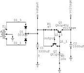
See Our actual Schematic here:
http://www.diyaudio.com/forums/attachment.php?s=&postid=1220544&stamp=1180393213
---------------------
🙂 1. Discussing this resistor: R1 = 2k2 and the optimal value of it.
I suggest and guess a rather low resistor value, maybe even like ~100 Ohm
which means 'only 6-7 mA' passing in Q3 MJE350 driver,
at the moment Q1 runs empty = no current into Q2 base.
Setting R1 to 2200 Ohm, will give a lowest current in Q3 of ~0.3mA (300uA)
which in my opinion is not good ( getting into non-linear Turn-On rgion of transistor ).
----------------------------------------------------
🙂 2. Try with a corresponding Resistor in upper output transistor.
From Q2 Base to Emitter. Emitter is at Output.
We can call this resistor R10 and having same value as R1
----------------------------------------------------
🙂 3. Values to try for R1 and R10.
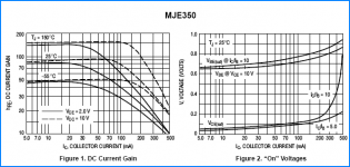
About: Q3, MJE350
..... is one TO126 transistor.
With cooling it can take a couple of watts. (Max rated 20Watt)
Safe opearating area (datasheet) of MJE350,
shows max 500mA at 20-30 Volt.
Temperature increase of cooled MJE350 is 6.25 C / watt.
At a room temperature of 30 C, we could allow say operation temp of 75 C.
75-30 = 45 C increase of temperature.
For using a 'safe value' of 15.0 C / Watt in a well cooled MJE350
we get:
3.0 Watt will give, 3x15 = 45 temp increase.
Roomtemp(30C) + 45 = Working temp = 75 C
This would not be too much! The ABSOLUTE max MJE350, TO126, can take is 150 C degreees.
MJE350 average working voltage is 20 Volt ( 50% of 40 Volt )
3.0Watt / 20 Volt =
Max 150mA Current at idle = Average.
🙂 Conclusion:
From a Temperature point of view an idle of 150 mA would be possible
----------------------------------------------------------------------------
😎 But our datasheet ( OnSemi ) tells us
that MJE350 works linear only upto max 100mA, at temp like 50-80 C
😎 See attached Figure of DC Current gain of MJE350.
Say Q1, lower 2N3055 runs at idle 1500 mA.
Say DC gain, HFE, is like ~50.
So Q1 needs maybe 1500/50= 30 mA into base, at average.
🙂
If we set Current in MJE350 to 70mA at idle, I think this will be a good value.
MJE350 will be working approximative:
70 +/-30 mA = between 40-100 mA
Even if this calculation uses DC Gain, the AC figures will be somewhat like this.
Maybe 70mA +/- 50 mA ( work within level 40-120mA at MAXIMAL OUTPUT POWER).
Now we normally DO NOT work amplifier at MAX
when we use it = Listen to music!!!
🙂
========================================
To set the working current of Q3 MJE350.
Target value: 70mA in Q3 at idle. (no music)
Q1 B-E Voltage: ~0.800 Volt
Q1 Base current: ~30mA
R1 current: ~40mA ( 0.040A )
Sum: 70 mA
R1 = 0.800/0.040= 20 Ohm
========================================
🙂
We make R1 = R10 = 22 Ohm
Each resistor connected between Q1 and Q2 (3N3055), Base - Emitter.
🙂
It is well worth test, with these values!
Lets see what this will result in.
If my Theoretical Calculations will match reality.
Thanks!
Regards
lineup
Lineup Audio Techniques
🙂
Datasheet MJE350 from OnSemi:
http://www.onsemi.com/pub/Collateral/MJE350-D.PDF
Attachments
Thanks Lineup your extra resistor helps with the problem as it will maintain the same difference between the ac currents no matter the required bias current for the outputs. The amount of imbalance changed with current through the driver regardless of the value of R1 ,example... 20mA through driver, R1 =1k, 100mA AC from Q1- 150mA AC from Q2...... 30mA through driver, R1=1k, 100mA AC from Q1- 170mA from Q2, with everything else being the same.
I think that the biggest problem is in the voltage gain stage. I didn't really notice it until I begin designing for a 20watt moster on a 54v rail. Non-symetrical slewing. So now since the output transistor only produce about 2/3's of the swing for each cycle, the transistor amplifying the slew limited half will naturally have less rms ac current. This is also why the imbalance changes for a given signal level.
In order to cure most of the problem, add Lineup's resistor from Q1 base to emitter the same value as R1, 1k is fine.
Next we make the amplifier much less efficient than it already is. We need to change R3 to lowest value that we can within the power limits of Q4.
First we decide our gain, with 35v rail a gain of 10 is fine but I would keep it below 16 so it doesnt become unstable. We set the gain by the ratio of R3 to R4. We need to keep R3 as low as possible, we will use 50ohms here. So now to get our gain of 10 we make R4 500ohms. So now we need to find our dc bias current for Q4.
We find this using (Vcc/2)/R4= (35/2)/500 = 35mA.
Now we need to note the voltage across R3. .035A*50ohms= 1.75v.
So our power dissipated by Q4 is ((Vcc/2)-voltage at R3)*Q4bias= ((35/2)-1.75)*.035= ~550mW
Our Q4 will be fine with a small tab heatsink.
Now the needed base current to get our bias current is needed. To find this we need to measure the beta of Q4, a DMM tester will work close enough.
Q4bias/Q4beta= IQ4base assuming a beta of 50, .018/50= 360uA.
We leave R5 100k.
We get the voltage across R5 = Voltage across R3 + .7=1.75+.7= 2.45 .
This gives a close enough value of the voltage at Q4 base and across R5. We now need to know the current diverted from the base of Q4 by R5.
VQ4base/100k= 2.45/100000= ~25uA
So we need R6+R7 to provide .00036+.000025= 385uA
Our value for R6+R7= Vcc-VQ4base/.000385= 35-2.45/.000385= ~85kohm
Then we will make R6 47kohm.
R7 then will be a 100kohm pot set to half it resistance for power up.
We can also find the max voltage swing easily using the simple principle that max current in a single transistor in class a is Iq*2.
Using the load resistor we have R4*Q4bias= 500*.035= 17.5v
At double the current we have R4*(Q4bias*2)= 500*(.035*2)= 35v
At 1mA,roughly before cuttoff, R4*Q4bias= 500*.001= .5v
So with the available voltage swing we see near rail to ground 34.5 volts peak to peak, but this isnt true.
Remember noting the voltage across R3? We can not swing more negative than this voltage.
The actual available swing is 35-.5-1.75= 32.75v peak to peak. Of course how much of it that is available on the output depends on bias.
So thats how to do the voltage stage relatively easy like, and if ive confused every one even further I cant help it.
I think that the biggest problem is in the voltage gain stage. I didn't really notice it until I begin designing for a 20watt moster on a 54v rail. Non-symetrical slewing. So now since the output transistor only produce about 2/3's of the swing for each cycle, the transistor amplifying the slew limited half will naturally have less rms ac current. This is also why the imbalance changes for a given signal level.
In order to cure most of the problem, add Lineup's resistor from Q1 base to emitter the same value as R1, 1k is fine.
Next we make the amplifier much less efficient than it already is. We need to change R3 to lowest value that we can within the power limits of Q4.
First we decide our gain, with 35v rail a gain of 10 is fine but I would keep it below 16 so it doesnt become unstable. We set the gain by the ratio of R3 to R4. We need to keep R3 as low as possible, we will use 50ohms here. So now to get our gain of 10 we make R4 500ohms. So now we need to find our dc bias current for Q4.
We find this using (Vcc/2)/R4= (35/2)/500 = 35mA.
Now we need to note the voltage across R3. .035A*50ohms= 1.75v.
So our power dissipated by Q4 is ((Vcc/2)-voltage at R3)*Q4bias= ((35/2)-1.75)*.035= ~550mW
Our Q4 will be fine with a small tab heatsink.
Now the needed base current to get our bias current is needed. To find this we need to measure the beta of Q4, a DMM tester will work close enough.
Q4bias/Q4beta= IQ4base assuming a beta of 50, .018/50= 360uA.
We leave R5 100k.
We get the voltage across R5 = Voltage across R3 + .7=1.75+.7= 2.45 .
This gives a close enough value of the voltage at Q4 base and across R5. We now need to know the current diverted from the base of Q4 by R5.
VQ4base/100k= 2.45/100000= ~25uA
So we need R6+R7 to provide .00036+.000025= 385uA
Our value for R6+R7= Vcc-VQ4base/.000385= 35-2.45/.000385= ~85kohm
Then we will make R6 47kohm.
R7 then will be a 100kohm pot set to half it resistance for power up.
We can also find the max voltage swing easily using the simple principle that max current in a single transistor in class a is Iq*2.
Using the load resistor we have R4*Q4bias= 500*.035= 17.5v
At double the current we have R4*(Q4bias*2)= 500*(.035*2)= 35v
At 1mA,roughly before cuttoff, R4*Q4bias= 500*.001= .5v
So with the available voltage swing we see near rail to ground 34.5 volts peak to peak, but this isnt true.
Remember noting the voltage across R3? We can not swing more negative than this voltage.
The actual available swing is 35-.5-1.75= 32.75v peak to peak. Of course how much of it that is available on the output depends on bias.
So thats how to do the voltage stage relatively easy like, and if ive confused every one even further
I cant help it.jerluwoo said:Thanks Lineup your extra resistor helps with the problem as it will maintain the same difference between the ac currents no matter the required bias current for the outputs.
The amount of imbalance changed with current through the driver regardless of the value of R1 ,example... 20mA through driver, R1 =1k, 100mA AC from Q1- 150mA AC from Q2...... 30mA through driver, R1=1k, 100mA AC from Q1- 170mA from Q2, with everything else being the same.
I think that the biggest problem is in the voltage gain stage.
.
>> I think that the biggest problem is in the voltage gain stage.
You Are Right, jerluwoo!
I would not call is 'a problem'
because this amplifier performs very well, the way it is. 😎
I prefer to call it main issue,
or most critical detail
... when we use no global FB.
It is usually very easy ta make buffers, follower, where no voltage gain ( GainV ~0.99 )
.. even at very high currents output ( Say 4.0-5.0 Ampere, RMS )
It is anywhere where we have a voltage gain we need to take extra care
... or add feedback correction.
The higher the voltage gain is ... the more care for everything

For example a RIAA Phono Amp
Requires many times a voltage gain of 500-1000 .......
You try to do this ... without Feedback 😀
Now, it can be done, and it has been done 😎
but you have to be a very clever boy or girl .... to do this.
Regards
lineup
🙂
No, we can hardly say this amp has got any problems to mention
not in the output part,
which, even if it is a simple folllower
has got plenty of local feedback.
Very good figures,
if we compare with other amplifiers with global feedback.
-----------------------------
I posted earlier in this thread a version of
my output stage in TRUE Class A, for this amplifier.
Fast Fourier analys:
http://www.diyaudio.com/forums/attachment.php?s=&postid=1037307&stamp=1161560554
Frequency Response and Phase analys:
http://www.diyaudio.com/forums/attachment.php?s=&postid=1037304&stamp=1161560122
My Comment to the FFT fourier was:
lineup said:🙂
Here is the fast fourier analysis of a 1 kHz signal
using this last version, restricted to 100 kHz upper freq limit.
We can see 2nd harmonic at -74dB is totally dominant.
3rd is very low at -113 dB
and 4th is also below -100dB, being at -103dB.
lineup
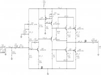
Ok,I'll call this my last post for this thread if no one else decides to build this amp (their loss for sure), and let this thread go to the archives. I highly recomend the following schematic using the transistors I did. The VAS transistor makes this amplifier, after trying several different to-220 cased types, I was very disappointed with the sound when I first built this one because the input transistors sounded bad and were unstable for the gain of 22 I wanted to use. Tell tell signs were drifting offset up and down, unusually warm vas trans, and slurred treble. So I was digging in my box of salvaged circuit boards, I like to keep boards from things that have many transistors and various parts, to experiment with. In comes a very nice little transistor, the Sanyo 2sd438. This transistor turned the sound of the amp into something wonderful. Super tight bass and crisp mids and treble, I was stunned at the difference. It is also stable at 22 gain, not sure why the to-220 types I tried were not, larger junction capacitances- not enough current to put them in a good operating point? Anyway for the simplicity you will not likely hear a better sounding amp for what little it would cost to build this one. The 2sd438 is obsolete now but there is an equivelent available from Fairchild semi ,ksc2316. This circuit sounds so much more powerful than the ~20 watts it puts out. Used with the simple power supply in the post above this one, you will have a nice little amp. Good luck to those who try it, I will post help if anyone wants it, but wont be adding anything further to this thread about configurations and the like. Happy DIY'ing.
Attachments
- Status
- Not open for further replies.
- Home
- Amplifiers
- Solid State
- My simple class a approach