You will like that cart, I like the top slightly bright and used 220pf 150k load. However 150pf 150k may be ideal.
I used mylar caps and implemented the subsonic filter on my board.
I am going to get an ML tip but the Conical is sounding really good.
I used mylar caps and implemented the subsonic filter on my board.
I am going to get an ML tip but the Conical is sounding really good.
Yes stocktrader200 , I am very curious to listen to it with some of my favorite records.
I read that after about twenty hours it stabilizes and sounds even better. We'll see.
Since you're talking about it, the next cartridge I would like to buy (later...), is the VM540ML (precisely, a Micro Line).
It too, in its price range (around 240 euros), seems to be a great cartridge, but certainly more demanding than the VM95C.
Vm540ML will require you to adjust the capacitance and also the load resistor.
47k 68k 100k and 47p.100p 150p 220p
As I am tuning my preamp for the Vm95 body , I will use the ML stylus for that cartridge.
47k 68k 100k and 47p.100p 150p 220p
As I am tuning my preamp for the Vm95 body , I will use the ML stylus for that cartridge.
Short update.
Revision 0.1b of MarcelvdG's circuit with High-Pass filter.


It seems pretty good to me.
What do you think?
Revision 0.1b of MarcelvdG's circuit with High-Pass filter.
- I added the 3x DIP switch to the schematic to select the input capacitance.
- I created a multiple footprint of the 2.2uF input capacitor, capable of accommodating most of the medium-sized polypropylene and film capacitors.
- The headers for the selection (via single Jumper) of the filter slope near the OP-Amp, are with 1.27mm pitch.
It seems pretty good to me.
What do you think?
Attachments

Hi mlloyd1 and MarcelvdG 🙂
Thanks a lot for checking.
Today I fixed small defects of the silkscreens, added the ground plane on the bottom and spaced the positive input pins (L and R) to 32 mm.
And this is also the recommended size for the RCA input connector holes on the rear panel, to keep the cable connection points very close.
I attach the last layout preview, then in the next few days I will prepare the files for printing.
The last SMD components ordered, should be available at JLCPCB in early May.
As soon as I have them all, I will proceed.

I was forgetting to say hello and thank arjen6t8 and twitchie too! 😉
Thanks a lot for checking.
Today I fixed small defects of the silkscreens, added the ground plane on the bottom and spaced the positive input pins (L and R) to 32 mm.
And this is also the recommended size for the RCA input connector holes on the rear panel, to keep the cable connection points very close.
I attach the last layout preview, then in the next few days I will prepare the files for printing.
The last SMD components ordered, should be available at JLCPCB in early May.
As soon as I have them all, I will proceed.
I was forgetting to say hello and thank arjen6t8 and twitchie too! 😉
Last edited:
I spent the last week at home, sick.
To distract myself, I worked a bit on the circuit suggested by Nick Sukhov with OPA2192 (Hi Nick!).
Its simplicity and the absence of THT components, make it a particularly interesting and compact design, which I tried to enhance with some tricks:
If you see errors or things that do not convince you, please report them.


To distract myself, I worked a bit on the circuit suggested by Nick Sukhov with OPA2192 (Hi Nick!).
Its simplicity and the absence of THT components, make it a particularly interesting and compact design, which I tried to enhance with some tricks:
- As in the MarcelvdG Circuit, I added Dip Switches (3x SPST) to set the input capacitance on eight possible values, from a minimum of 15pF to 144pF.
- The new board measures 42 x 45 mm. while the distance between the positive input pins is about 30 mm.
- The dual power connector now has a double footprint, 3.5 mm. and 2.54 mm.
- The input and output connectors J1, J2, J3, J4 (as well as the secondary footprint of the power connector) are all blocked in a 100 millimeters grid. In this way it is possible to interface this board with any "thousand hole" prototyping board, with a 2.54 mm pitch, only using normal 2.54 mm "Header/Socket" connectors.
If you see errors or things that do not convince you, please report them.
Attachments
I discover now that after a few minutes it is no longer possible to edit the posts.
By mistake, I wrote "100 millimeters grid" instead of "100 mills grid".
By mistake, I wrote "100 millimeters grid" instead of "100 mills grid".
There is normally a limit of 30 minutes for editing, except for post #1, which can be edited indefinitely.
Hi MarcelvdG,except for post #1, which can be edited indefinitely.
Interesting, I didn't know that.
Hi MarcelvdG,
Interesting, I didn't know that.
I was on this forum for 17 years without knowing that 😉 It's handy when threads get long, you can then add links to the most relevant posts to post #1 as an overview.
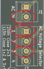
Another short update, which concerns the power stage that I will use for the RIAA Preamp.
In order to facilitate fixing and connections, I prepared a PCB to interface the Talema 25VA Encapsulated Transformer (code 70063K), for which I also had to create a new Footprint.
To take advantage of all the features of the transformer (such as the double primary winding), I have:


If you think it can work and that it does not require other changes, give me a "Go - no - Go", so I can also attach the Gerber files.
I think it could be useful to anyone who wants to use a 25VA encapsulated Talema, regardless of the output voltage.
In order to facilitate fixing and connections, I prepared a PCB to interface the Talema 25VA Encapsulated Transformer (code 70063K), for which I also had to create a new Footprint.
To take advantage of all the features of the transformer (such as the double primary winding), I have:
- Implemented the possibility of setting the AC input voltage (115V or 230V) through wire jumpers (or soldering them directly to the pads).
- Added a double output connector for the Secondaries, to have an output on both the front and rear side (but of course only one must be used).
- All connectors have a 5.08 mm pitch.
If you think it can work and that it does not require other changes, give me a "Go - no - Go", so I can also attach the Gerber files.
I think it could be useful to anyone who wants to use a 25VA encapsulated Talema, regardless of the output voltage.
Attachments
Have you ever heard about creepage distance for line voltage AC on PCB? Make the distance between tracks carrying line AC voltage about the same it's on transformer. I.e. around 200 mil/5mm. Making slots between the J2 connector's pads would not be bad either.I prepared a PCB to interface the Talema 25VA
Attachments
Hi Alexberg,
Thanks for the heads up.
What exactly do you mean by: "Making slots between the J2 connector's pads"?
Is it a little better this way?

Thanks for the heads up.
What exactly do you mean by: "Making slots between the J2 connector's pads"?
Is it a little better this way?
Slot allows to increase creepage distance i.e. conductor spacing along the surface. Clearance on the other hand is the one through the air (line of sight).
Hi Alexberg,
Thanks, now I understand the difference between creepage and clearance. 😉
Considering the low currents involved, do you really think it is necessary to create slots between the pads of the J2 connector?
Hi arjen6t8,
Thanks for the suggestions, I completely agree.
Meeting the electrical requirements is much more important than adding an optional connector.
Schematic and PCB updated to version 0.2

There is still a single crossing of traces between the primaries (top/bottom).
Could it still be okay?
Thanks, now I understand the difference between creepage and clearance. 😉
Considering the low currents involved, do you really think it is necessary to create slots between the pads of the J2 connector?
Hi arjen6t8,
Thanks for the suggestions, I completely agree.
Meeting the electrical requirements is much more important than adding an optional connector.
Schematic and PCB updated to version 0.2
There is still a single crossing of traces between the primaries (top/bottom).
Could it still be okay?
Attachments
In this latest version I tried to keep the traces out of the transformer area, but the one from Pin 3 of TR1 to the J1 remains present, (with only one crossing).

This trace could also be moved out of the TR1 area, but with two crossings, like this.

This trace could also be moved out of the TR1 area, but with two crossings, like this.
Last edited:
- Home
- Source & Line
- Analogue Source
- My OPA1656 RIAA PreAmp (one more)