As it has been pointed out earlier, spice (or EWB as I'm using) doesn't take component variations into account (except for resistors, but unless you have a really fast computer it takes way too long to simulate using eg. 1% or 5% resistors instead of ideal ones), and probably because of this, measuring a circuits performance using these programs isn't too close to real-life, but here goes...
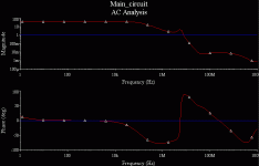
The attached graph shows the AC response of my circuit with current mirrors. Simulated THD is 0.004% and no DC offset.
The attached graph shows the AC response of my circuit with current mirrors. Simulated THD is 0.004% and no DC offset.
Attachments
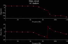
This graph is for my circuit with resistors instead of current mirrors. After playing with different resistor values I got a THD of 0.003%, however, the DC offset is a massive 9.2 Volts!
This is probably because I had to use a higher value degeneration resistor on the upper differential pair (1.5 kOhm) than the lower diff (330 Ohm). Should I just put a cap on the output rail and pretend it's not there, or is there anything to do about it?
This is probably because I had to use a higher value degeneration resistor on the upper differential pair (1.5 kOhm) than the lower diff (330 Ohm). Should I just put a cap on the output rail and pretend it's not there, or is there anything to do about it?
Attachments
Hi,
can you post the resistor version of the schematic?
Is it possible to add operating voltages and/or operating currents to the schematic?
Can you change the vertical scale (phase angle) of the phase plot? try 100degree to -300degrees instead of 100degrees to -100degrees.
can you post the resistor version of the schematic?
Is it possible to add operating voltages and/or operating currents to the schematic?
Can you change the vertical scale (phase angle) of the phase plot? try 100degree to -300degrees instead of 100degrees to -100degrees.
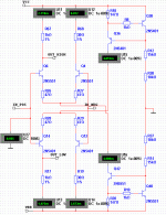
Here's the resistor version (only showing the input stage, the rest is the same). The two displays on the left side are voltmeters, while the right displays are (milli)ammeters. The value of the resistors on the right leg of each diff pair didn't affect the performance, so I just kept the 30 Ohm degeneration resistors of the original version.
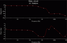
I tried adjusting the current source setting the tail current for the lower diff pair, so that both pairs would get the same tail current. This reduced the DC offset somewhat (from 9.2 Volts to 8.1 Volts), but it also increased the THD to more than 1%.
Not sure how to change the scales on the graphs, but I'll look into it 🙂
Attachments
something seriously wrong.
1.) the model for the 2N CCS devices is throwing up 668 & 721mVbe. Far too high.
2.) why the different values for R17 & R67
3.) what voltage is across the VAS, Vbe?
post more of the schematic and a lot more I & V values.
PS
Forget distortion until you have learned how to get the sim to give out sensible answers to your questions.
1) According to the datasheet (and mr. Slone) the Vbe for these transistors should be approx 0.67 Volts, why is this too high?
2) any other value than 330 Ohms for R17 and anything below 1.2 kOhms for R67 makes the output signal warped and heavily distorted (simulated THD is over 30% if I set both to 1k, for instance).
3) will take a look at it when I get home from work 🙂
2) any other value than 330 Ohms for R17 and anything below 1.2 kOhms for R67 makes the output signal warped and heavily distorted (simulated THD is over 30% if I set both to 1k, for instance).
3) will take a look at it when I get home from work 🙂
according to the Fairchild 5551 datasheet you can expect 500mVbe to 650mVbe for our typical currents and temperatures. @ 5mA I see 500mVbe to 700mVbe for the temperature range of 125degC down to 25degC.
I do not believe a model that suggests 668 to 721mVbe for your operation.
There is something seriously wrong with the operation of the circuit.
Forget distortion and start examining the voltages and currents in the sim to understand what it is you have simulated.
PS,
it is no good if you don't understand what the sim is doing for you.
You should be able to do most of the calculations yourself to be able to check that the sim is throwing out sensible answers. It's standard software rules. CHECK the OUTPUT manually before relying on the computer generated rubbish.
I believe EWB uses the Vbe/IC-curve at 25 degrees in it's calculations, so it shouldn't be too far from the truth (I measure the same values on the real, breadboarded version).
and when it comes to calculations, I'm not too good at anything beyond Ohm's and Kirchoff's laws, and anything that can be extracted from the datasheets. But I'm learning!
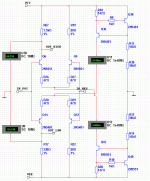
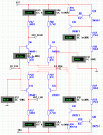
Here's the input stage with the same resistor value on the upper and lower diff pair legs. These measurements where made in the amplifiers quiescent state, with no signal applied. I find it odd that theres a DC voltage of -0.6 Volts at the input, especially since it's connected to ground (through a 100K resistor).
and when it comes to calculations, I'm not too good at anything beyond Ohm's and Kirchoff's laws, and anything that can be extracted from the datasheets. But I'm learning!
Here's the input stage with the same resistor value on the upper and lower diff pair legs. These measurements where made in the amplifiers quiescent state, with no signal applied. I find it odd that theres a DC voltage of -0.6 Volts at the input, especially since it's connected to ground (through a 100K resistor).
Attachments
...And the VAS, with lots of voltage meters... now's the time to get concerned about high Vbe values, take a look at Q13 and Q16! Apart from that, I believe the signal voltages to be as expected (but no, I haven't done any calculations) due to the dc offset at the input.
Attachments
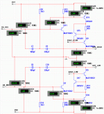
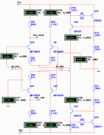
and finally part of the output stage (the whole stage won't fit in an image that this forum will accept, but the rest can be seen in an earlier post). R22 should be a potmeter, but it's easier to use a resistor with selectable value than a potmeter in the sims.
I believe the problem could be related to the DC offset at the input? If I disconnect the 100k resistor from the input transistors, the DC offset increases to -1.5 Volts. If I then disconnect the bases of the two input transistors from each other, I measure approx 200 mV at the base of Q14 and 300 mV at the base of Q6, and the voltages throughout the VAS and the output stage is quite symmetrical. Does this mean anything? Is it possible for current to flow from the base of a transistor to the base of another transistor?
edit - connected an ammeter between the base of Q14 and Q6, and measured 0.02 mA flowing from Q6 to Q14
Attachments
Hi,ventle said:
and when it comes to calculations, I'm not too good at anything beyond Ohm's and Kirchoff's laws, I find it odd that theres a DC voltage of -0.6 Volts at the input, especially since it's connected to ground (through a 100K resistor).
now calculate the current in that 100k grounding resistor.
Ohm's law : I=0.6/100e3=6uA. this is the input offset current. Look up a bjt opamp datasheet and you'll see similar values.
Now look at the four currents in the collector loads of the two Long Tail Pairs. Are they matched? No. Look at the emitter currents in the degeneration resistors. Adjust the collector loads to match these Ire currents exactly.
Each pair total should be similar to the CCS current.
Now adjust the 147r with the higher current. Increase it until the CCS reduces to match the current in the other CCS.
Now go back and look at the new Ire values. What happened. Are you starting to understand what the LTP is doing. Nothing more than Ohm's law, but hopefully you are stating to ask the sim the right questions and understanding WHY it gives those answers.
Look back at the new input offset current. Has it changed? Why?
Can you estimate the gain (hFE) of each of the LTP transistors?
What do you need to check all four transistors?
What would happen to input offset current and input offset voltage if you substituted proper (more suitable) input transistors for the 2n devices you have at present?
Finally, what is the voltage on the inverting input?
Are you ready to start investigating the next stage of your amp?
I'll leave you to get on with it.
If you have confirmed these voltages in your BB then the model is good. I'm just surprised @ such high values of Vbe.ventle said:I believe EWB uses the Vbe/IC-curve at 25 degrees in it's calculations, so it shouldn't be too far from the truth (I measure the same values on the real, breadboarded version).
I would suspect some instability, oscillations.
But I am not sure what causes it.
I noticed one detail.
Those 1 k resistors in the VAS compensation network.
They are connected to GND in original circuit.
Not to V+ and V-
I am talking about R9 and R11 in this attachment:
http://www.diyaudio.com/forums/attachment.php?s=&postid=1563396&stamp=1216235702
Also in Slone circuit is one 100uF cap, C13 across VBE multiplier.
I can not see it in your schematic.
http://www.diyaudio.com/forums/attachment.php?s=&postid=1563398&stamp=1216235920
But, neither of these 2 points, should really be causing some instability problems, I think.
===============================
This measurements is REALLY STRANGE.
http://www.diyaudio.com/forums/attachment.php?s=&postid=1563390&stamp=1216235451
On the top you read
U11 = 2.719 mA
U12 = 0.012 A = 12 mA
Now, as the CCS is feading 4.918 mA,
where does 'the extra' 9-10 mA come from ????????
It is such figures, that can make you suspect some oscillations ( AC-Currents ) going on.
One thing is special
is the VAS cascoding transistors are following the output
by BIAS_HIGH and BIAS_LOW.
You are using MJE15032/33 for these cascodes.
Can you try with some faster transistors?
Like MJE340/350.
BD139/140 maybe can not be used ( 80 Volt max )
----------------------------
edit:
I your VAS stage here
http://www.diyaudio.com/forums/attachment.php?s=&postid=1563396&stamp=1216235702
... you are Using MJE15032/33 to drive 2N5401/5551 ( Q11, Q13 and Q7, Q16 )
Normally, I would expect the other way ...
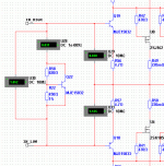
So many questions 🙂 well, first, to Andrew's post, here's what I came up with after tweaking the input stage (see attachment). I think this is as close as it'll get to being balanced. If I change R67 to make the upper pair balanced, this will make the lower pair unbalanced, and vice versa.
I chose the values of R68 and R19 by just doing som trial and error... not sure if there's some better values to be chosen here, seems like they have very little effect on the stage performance.
Yes, the input offset current changes, and I believe the point you are trying to make here is that it's due to the (nearly) balanced quiescent currents in the upper and lower LTP...
How would I deal with current imbalance issues in real life? Replace R17, R67 and R20 with potmeters?
The base of Q6 draws 0.012 mA and it has a collector current of 2.231 mA. hfe should then be 2.231/0.012 = 186?
Learning from mr. Slone, I thought the 5401/5551 were quite good as input transistors... which ones would you suggest instead? Are MPS8099/MPS8599, as he has used in the opti-mos design, better ones?
... will look deeper into the VAS when I get home from work.
lineup:
this circuit is not based on the opti-mos, but on his "optimum amplifier" (page 328 in the "high-power audio amplifier construction manual"), where the 1k resistors are connected to the supply rails. Now I might be wrong on this, but doesn't both the earth ground rail and the supply rails work as signal (AC) ground, meaning it doesn't really matter which one of these they're connected to?
Cap across Vbe multiplier was omitted becaus it seemed to be causing oscillations... will get back to this when anything else seems to be working.
...and about the strange measurements: there are some short-lived oscillations upon startup. It may have happened that I didn't wait for those oscillations to cease before I captured the screenshot
Attachments
ventle said:
... will look deeper into the VAS when I get home from work.
lineup:
this circuit is not based on the opti-mos, but on his "optimum amplifier" (page 328 in the "high-power audio amplifier construction manual"), where the 1k resistors are connected to the supply rails. Now I might be wrong on this, but doesn't both the earth ground rail and the supply rails work as signal (AC) ground, meaning it doesn't really matter which one of these they're connected to?
Yes, those MJE150xx TO-220 driving 2N5xxx TO-92, in VAS ......
You have probably made a mistake with those, when setting up your VAS circuit for simulation.
And about GND vs. Supply rails, you are correct.
They should work as good as, in this case for those 1k resistors.
So, the problem should not be there.
Yes, those MJE150xx TO-220 driving 2N5xxx TO-92, in VAS ......
You have probably made a mistake with those, when setting up your VAS circuit for simulation.[/B]
Actually, I too thought this was the wrong order of the darlington pairs, but this is actually how Slone has done it (except he uses 2SB649/2SD669 as the drivers. I'm using 2SA940/2SC2073, but EWB doesn't have models for these, and they're quite similar to MJE15032/15033). So it's not a mistake according to the schematics, but it might still be a mistake 🙂
So, if I remember the school lessons correctly, to take full advantage of a darlington pair, the first transistor (the one that gets the signal from the input stage) should be a transistor with high beta (in this case the 2N-transistors), while the second one (that feeds the output stage) should be capable of sourcing/sinking high currents/dissipating more power... correct?
I did have some measurements to post now, but I'll look into the transistor misplacement first...
- Status
- Not open for further replies.
- Home
- Amplifiers
- Solid State
- My Mosfet amp: why isn't it working?