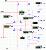
So, here's the VAS with probably a more "correct" layout (wrt the darlington pair), so let's see what I do understand and don't understand:
- the compensation network (C7 through C10, R9 and R11) does not affect quiescent conditions
- the relationship between the base currents and collector currents equals the hfe of Q13 and Q16. This calculates to 213 for both transistors. Is this odd, when the hfe for the same transistors used in the LTP was 186? Or is this quite as expected when the collector currents increase? Datasheets suggest a hfe between 150 and 225 for the 5551 and 100 to 140 for the 5401. Should I mistrust the spice model after all?
- the Vbe of Q7 and Q11 across resistors R13 and R15 sets the quiescent current through transistors Q13 and Q16 (the value of R15 was tweaked to establish balance, if this is a goal...)
- Q15+R30 and Q17+R31 are used for limiting the current through Q11+Q9 and Q5+Q7. In other words, a simple protection method.
- Q9 and Q5 sets the quiescent current through Q11 and Q7 using the bias voltages provided by the output stage (not really sure on this one - anyone care to confirm or correct this?)
- the voltage between the out_high and out_low connectors are decided by the Vbe multiplier in the output stage. What I don't understand is why there's a negative DC offset here? Do I need to investigate the output stage to find the problem?
edit - the in_pos voltage is approx 100 mV higher in absolute value (closer to the supply rail) than the in_neg voltage. Because the output signal is taken from the collector of the darlington pair, the VAS stage is inverting it's input signal, right? And because of this, the +100 mV DC offset at the input of the VAS is amplified to a -5 Volt DC offset at the output? Or am I completely off track now?
Attachments
Looks better.
And now the Q9 MJE15033 is cascoding Q11 MJE15033.
this makes more sense.
-----------------------------------------
I remember this amplifier by Randy Slone has been discussed several times before.
And some have questioned if the VAS will actually work.
I do not know ....
One old topic:
Unstable VAS current in amp from Slone book
http://www.diyaudio.com/forums/showthread.php?threadid=16796
Here is the google search, to find similar diyaudio.com topics:
Search diyAudio - Slone Amplifier Construction Manual
Lineup
See also this post
by lumanauw
I think he is refereing to the same amplifier schematic you build:
http://www.diyaudio.com/forums/showthread.php?postid=263668#post263668
http://www.diyaudio.com/forums/attachment.php?s=&postid=263668&stamp=1068623354
by lumanauw
I think he is refereing to the same amplifier schematic you build:
http://www.diyaudio.com/forums/showthread.php?postid=263668#post263668
Here is his attached Slone schematic Figure 10.3lumanauw said:
But when I make experiment of it, this design just doesn't work.
Up until now I cannot figure what is the voltage in the base of Q11 and Q12 (first VAS transistor). I need it to determine the VAS's standing current. But the base of Q11 and Q12 is located between collector of differential and collector of current mirror. How can I calculate the voltage between 2 collectors?
When I just change the current mirror with ordinary resistor, this amp work. But how come the author have measurement figures, if the amp doesn't work?
http://www.diyaudio.com/forums/attachment.php?s=&postid=263668&stamp=1068623354
Read those thread when homemodder advised me to on the previous page 🙂 the amplifier won't work as long as it has current mirrors on the input LTPs, so now I'm just experimenting on trying to make it work properly with only resistors connected to the collectors of the LTP transistors.
And you are absolutely right, that figure 10.3 is the one I've been using as reference.
And you are absolutely right, that figure 10.3 is the one I've been using as reference.
In that figure 10.3 deoesn't he use 10k for the input resistance
and the feedback resistance ? Perhaps the 10k that Sloan uses
might provide a better path for the input stage bias currents than
the 100k you use. I am refering to the curent the bases of the input transistors draw.
and the feedback resistance ? Perhaps the 10k that Sloan uses
might provide a better path for the input stage bias currents than
the 100k you use. I am refering to the curent the bases of the input transistors draw.
that might be true. I was hoping that I could build it with 100k input resistance, because this would fit the preamp circuit better, but I'll take a look at if using 10k will be better.
Still, waiting for anyone to suggest better/more suitable transistors to use in the input stage than the 2N5401/2N5551... are MPS8099/MPS8599 good ones? At least their beta value is way higher (over 300 compared to about 180 for the 2N ones)...
Still, waiting for anyone to suggest better/more suitable transistors to use in the input stage than the 2N5401/2N5551... are MPS8099/MPS8599 good ones? At least their beta value is way higher (over 300 compared to about 180 for the 2N ones)...
simulate first
Maybe you made a mistake with the wiring of the devices, an easy trap with mosfets.
Maybe you made a mistake with the wiring of the devices, an easy trap with mosfets.
Hi,ventle said:waiting for anyone to suggest better/more suitable transistors to use in the input stage than the 2N5401/2N5551... are MPS8099/MPS8599 good ones? At least their beta value is way higher (over 300 compared to about 180 for the 2N ones)...
the amp and the simulation will work with the low beta devices.
Note how close the voltage is between the inverting input and the non-inverting input.
BC5xxC are hFE of 420 to 800 (2n5551 hFE 80 to 250). Many specialised transistors can exceed this by a large margin. I suggest you select a lowish noise, hFE~500 and fT~200MHz for the input transistor.
The two outputs on the LTP collectors inject and sink current to the pair of VAS transistors.
This current unbalances the LTP.
You must check the emitter currents to see what quiescent current is flowing through the LTP transistors.
- Status
- Not open for further replies.
- Home
- Amplifiers
- Solid State
- My Mosfet amp: why isn't it working?