Unless you are running to hot for reliability then changing the heatsinks won't gain you anything. It won't help with DC drift, just slow it down.
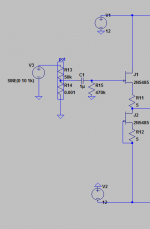
The value of R4 depends on how you implement the servo. If its light acting then you make it as high as high a value as possible that would still allow the offset to be corrected.
You can add a light acting servo to the original design by simply splitting R19 into two equal values and feeding the servo correction voltage to the junction of the split. That keeps the original board intact and the servo is just a small add on.
Unless you are running to hot for reliability then changing the heatsinks won't gain you anything. It won't help with DC drift, just slow it down.
The value of R4 depends on how you implement the servo. If its light acting then you make it as high as high a value as possible that would still allow the offset to be corrected.
You can add a light acting servo to the original design by simply splitting R19 into two equal values and feeding the servo correction voltage to the junction of the split. That keeps the original board intact and the servo is just a small add on.
So, 470K on the DC-servo output, something like 1Meg on the input. Replacing R19 with 2x 100K in series using the midpoint to inject signal from DC-servo.
The cap + series resistor test first I assume?
Thanks alot for all help, it's greatly appreciated 🙂
Thanks alot for all help, it's greatly appreciated 🙂
You're very welcome 🙂
For the servo, think of it like this... the opamp can swing between say - and + 10 volts. So you have that range of voltage that is available to be applied for correction via a resistor to the input of the amp.
With the servo not connected, lets say the amp can be trimmed to around zero volts offset at Q3 emitter when its hot and been on a while.
When the amp is cold, you might find the offset is -200 mv.
So we have an approximate range of values to work with. You need to correct at least -200mv offset and yet the amp could perhaps reach +150mv offset when really hot and its been on for hours on a hot day.
So you could find a value for R4 by trial and error simply by connecting a resistor from the point where the correction will be applied to first the positive rail, and then the negative rail. The resistor you choose should be able to swing the offset from say -300mv when connected to one rail thorough to -300mv when connected to the other rail. That would ensure the opamp could always pull the offset to zero.
The cap and resistor test is just for interest really, but if you see a voltage appear then its because the rails are altering slightly.
I've just replaced the 220K with two 100K in series. I brainf*rted slightly there as I was shure it was 200K without double checking.You're very welcome 🙂
For the servo, think of it like this... the opamp can swing between say - and + 10 volts. So you have that range of voltage that is available to be applied for correction via a resistor to the input of the amp.
With the servo not connected, lets say the amp can be trimmed to around zero volts offset at Q3 emitter when its hot and been on a while.
When the amp is cold, you might find the offset is -200 mv.
So we have an approximate range of values to work with. You need to correct at least -200mv offset and yet the amp could perhaps reach +150mv offset when really hot and its been on for hours on a hot day.
So you could find a value for R4 by trial and error simply by connecting a resistor from the point where the correction will be applied to first the positive rail, and then the negative rail. The resistor you choose should be able to swing the offset from say -300mv when connected to one rail thorough to -300mv when connected to the other rail. That would ensure the opamp could always pull the offset to zero.
The cap and resistor test is just for interest really, but if you see a voltage appear then its because the rails are altering slightly.
Should I redo the operation using 2* 110K resistors (if I find some in my stores?
I'll use "sockets" for the input resistors in the DC-servo circuit then, so that I'll be able to swap them easy enough.
I tried powering on the jfet headamp on the breadboard again having changed the temporary supply to one bridge rectifier using center tap as GND.
That didn't work either.
Tested measuring resistance between secondaries and secondary to center tap.
Between windings: 2.2R
Winding to center tap: 1.6R
As I have a bunch of PTP solder supports, I'm thinking of adding one to the MDF board acting as star GND connecting to PE pin on the IEC socket.
Is that OK numbers?
It's an EI type transformer.
I have not connected the "body" of the transformer to PE GND. Maybe that is why it's acting up?
Since transformer, vregs and headamp are all screwed to a piece of MDF there's no other connection from transformer to GND.
Two 100k's are absolutely fine. You then tweak the offset preset pot to get as close to zero volts as you can at the main amp output, then you couple the servo to the junction of the 100k's and you should see the offset snap to zero volts instantly. The resistor to tweak is the one from the output of the opamp, the input one stays at 1 meg (or higher)
So this is another project then...
Is this a power supply problem you have... would have to see the circuit but the best check of the transformer is just to confirm the output voltages are OK across the windings. If you suspect the rest of the circuit is dragging things down then do the check off load with the secondary's disconnected.
I tried powering on the jfet headamp on the breadboard again having changed the temporary supply to one bridge rectifier using center tap as GND.
So this is another project then...
Is this a power supply problem you have... would have to see the circuit but the best check of the transformer is just to confirm the output voltages are OK across the windings. If you suspect the rest of the circuit is dragging things down then do the check off load with the secondary's disconnected.
Two 100k's are absolutely fine. You then tweak the offset preset pot to get as close to zero volts as you can at the main amp output, then you couple the servo to the junction of the 100k's and you should see the offset snap to zero volts instantly. The resistor to tweak is the one from the output of the opamp, the input one stays at 1 meg (or higher)
Ah, I'll have to re-work the DC-servo board slightly then as I made the 1Meg resistors swappable and the 470K resistors soldered in place.
Soldered the wires from the PCB, but not yet to the DC-servo board.
This is the project I started the thread about.So this is another project then...
Is this a power supply problem you have... would have to see the circuit but the best check of the transformer is just to confirm the output voltages are OK across the windings. If you suspect the rest of the circuit is dragging things down then do the check off load with the secondary's disconnected.
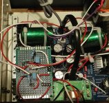
Tried with the R-Core in the JHL clone chassis and LT1083 vregs.
With the changes made to the jfet buffer I got around 1.4vdc offset, slightly better than before. I had not put the suggested 10K to GND as suggested though as I ran out of time for diy.
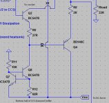
Also noted that on the right channel, the CCS's got hot, but on the left channel the non-ccs BJT's got very hot.
Attachments
So on the FET buffer... if there is a difference in temp between the two channels then that can only be one (or combination) of two things. The CCS currents are unequally... which is unlikely if the correct current defining resistors are used, and secondly, the DC voltages are different perhaps due to imbalance in the FET's. That's more likely, and a small difference in voltage across one or other of the CCS transistors would appear to make it run hotter (and its partner cooler) than the ones in the other channel.
So on the FET buffer... if there is a difference in temp between the two channels then that can only be one (or combination) of two things. The CCS currents are unequally... which is unlikely if the correct current defining resistors are used, and secondly, the DC voltages are different perhaps due to imbalance in the FET's. That's more likely, and a small difference in voltage across one or other of the CCS transistors would appear to make it run hotter (and its partner cooler) than the ones in the other channel.
I'll re-work that part of the board, the CCS's.
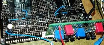
The strange thing is that the CCS to the far left in the pic is the one getting hot for that channel, and none of the CCS's on the other channel but the two BJT's between them. (As seen in the pic in my previous post)
Probably best to show it as a circuit diagram really, and point out 'this ones hot', 'this one is cold' etc together with voltage readings ... circuits make sense 🙂, pictures much less so because you are the only familiar with the layout 😛
Probably best to show it as a circuit diagram really, and point out 'this ones hot', 'this one is cold' etc together with voltage readings ... circuits make sense 🙂, pictures much less so because you are the only familiar with the layout 😛
Very true, my bad 😱
I'm suddenly not sure about the value of the resistors used between 1uF and the 2SK170's (shown as other fets in schem), and the vol-pot is not attached to the circuit yet.
The DC-Servo is removed from the circuit for now, and was incorrect anyway IIRC.
Soo, for one channel the top CCS (Q5, Q6)gets warm, not alarmingly so though.
For the other channel Q1 and Q2 gets HOT, barely able to touch them after <5min of being powered on.
I've only tested the circuit with +/-12Vdc so far.
Attachments
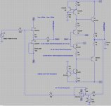
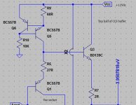
Q5/Q6 and Q7/Q8 should be equally hot as long as the following conditions apply.
1/ The 68 ohms that define the currents are correct and equal in both upper and lower CSS.
2/ The voltage on Q5 and Q8 collectors should be equal and 'opposite'. If you have significant DC offset (the output is not at zero) then that means Q5 and Q8 will have different voltages across E-C. Although the currents should be equal, the one with the highest differential across it will run hottest.
Everything is about symmetry on this type of circuit. The base current into Q3 and Q4 should be approximately equal and be a very small percentage of the current available from Q5 and Q6.
If you remove the final output transistors Q3 and Q4 then the circuit should settle to a symmetrical condition with equal dissipation in upper and lower halves. Once you get an imbalance of more than a couple of volts then that starts to become noticeable in temperature changes between upper and lower halves.
If the two channels are very different in terms of temperatures then you need to go back to the basics and measure the current flow in each CSS and see where the problem is... because something must be different to reflect as a higher operational temperature.
Q5/Q6 and Q7/Q8 should be equally hot as long as the following conditions apply.
1/ The 68 ohms that define the currents are correct and equal in both upper and lower CSS.
2/ The voltage on Q5 and Q8 collectors should be equal and 'opposite'. If you have significant DC offset (the output is not at zero) then that means Q5 and Q8 will have different voltages across E-C. Although the currents should be equal, the one with the highest differential across it will run hottest.
Everything is about symmetry on this type of circuit. The base current into Q3 and Q4 should be approximately equal and be a very small percentage of the current available from Q5 and Q6.
If you remove the final output transistors Q3 and Q4 then the circuit should settle to a symmetrical condition with equal dissipation in upper and lower halves. Once you get an imbalance of more than a couple of volts then that starts to become noticeable in temperature changes between upper and lower halves.
If the two channels are very different in terms of temperatures then you need to go back to the basics and measure the current flow in each CSS and see where the problem is... because something must be different to reflect as a higher operational temperature.
This is what I was thinking, something is not as it should in the Diamond buffer circuit.
I'll re-work it and while I'm at it put slightly less overkill heatsinks on the BD139/BD140's lol.
I have a bunch of BD139/BD140's with B and Vf written on them, maybe swap the ones on board to some with as close of the above numbers as I can find?
Could spend an hour or two measuring BC547/BC557 or BC550/BC560's as well to get some with close numbers?
measure ther voltages around the CCS
Vr9
Vbeq5
Vr10
these Vbe should read ~600mVdc to 700mVdc
Vr10 ~{12-2*Vbe} = ~10.7Vdc
Calculate the current through R9 (Ir9).
Measure Vr5 and calculate Ir5
Base current of Q3 + Ir5 ~= Ir9
Repeat this check for the -ve half CCS
Vr9
Vbeq5
Vr10
these Vbe should read ~600mVdc to 700mVdc
Vr10 ~{12-2*Vbe} = ~10.7Vdc
Calculate the current through R9 (Ir9).
Measure Vr5 and calculate Ir5
Base current of Q3 + Ir5 ~= Ir9
Repeat this check for the -ve half CCS
I have a bunch of BD139/BD140's with B and Vf written on them, maybe swap the ones on board to some with as close of the above numbers as I can find?
Could spend an hour or two measuring BC547/BC557 or BC550/BC560's as well to get some with close numbers?
I'm not so sure that matching bjt's will gain you anything here. Any differences due to mismatch should be minimal among devices of the same type number, certainly as far as defining the CCS currents and so on.
I'm not so sure that matching bjt's will gain you anything here. Any differences due to mismatch should be minimal among devices of the same type number, certainly as far as defining the CCS currents and so on.
Replaced the 0805 resistors with 0.4w vishay's.
The un-even heat problem seems to have been solved, I think one of the CCS resistors (in the neg rail CCS feeding the bottom BJT's, the channel having very hot Q1&Q2).
DC offset still over 1.6Vdc though.
Too tired to do any more diy today.
Well, despite it's difficulty to get stable, I've started working on a AD797 based input board for the diamond buffer.
The FFT looks OK I think, alot better than the Jfet buffer FFT did.
I dropped the supply to +/-10Vdc and the output resistors of the BD139/BD140 to 1R5 from 2R15.
I'll use DIP8 sockets so that I can easily swap single opamps.
The FFT looks OK I think, alot better than the Jfet buffer FFT did.
I dropped the supply to +/-10Vdc and the output resistors of the BD139/BD140 to 1R5 from 2R15.
I'll use DIP8 sockets so that I can easily swap single opamps.
Attachments
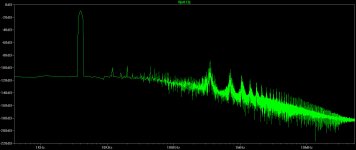
You might find opamp models a bit optimistic in their distortion results and FFT profile although whatever you are using for the AD797 is at least giving something in the way of realistic results.
This is from a non inverting op-amp buffer circuit that I developed.


This is from a non inverting op-amp buffer circuit that I developed.
- Status
- Not open for further replies.
- Home
- Amplifiers
- Headphone Systems
- "My" first design headamp, DC-servo question