I am in an electronics class in college and I am working on a headphone amp for my final project. The class is the first electronics class, so I need to stick to something fairly simple. I need to be able to analyze the entire circuit by hand, so nothing really complicated. I am thinking of a simple voltage follower with no voltage control since it will be used mostly with my computer. How does this look to you guys? Am I doing anything terribly stupid? Any simple changes that would improve things? I know the circuit seems trivial, but I am pretty new at this.
Vdd = 15V
Id = ~300mA
Vdd = 15V
Id = ~300mA
Attachments

May I suggest that you read this thread?
http://www.diyaudio.com/forums/pass-labs/66822-sewa-seven-watt-amplifier.html
http://www.diyaudio.com/forums/pass-labs/66822-sewa-seven-watt-amplifier.html
Hi,
you have shown a CCS loaded, source follower, in single ended mode, powered from a single polarity PSU.
The maximum current available from the follower <bias current.
That bias current flows through your current mirror.
Check your current mirror dissipation.
Check the high pass filter at the input of the amplifier.
PS.
I don't think the SEWA is an example that should be followed.
Last edited:
I originally used a dual polarity PS thinking that if I found that I needed gain I could add a simple op-amp front end with modest gain. Then, when I modeled the amp without the negative PS the performance was almost identical, so I figured I would get rid of the negative rail. Is there any reason I am missing to stick with a dual supply?
The SEWA is interesting. Don't those biasing zeners constitute a positive feedback loop? In small signal won't they appear as small resistors? Also, what is the purpose of the shunt resistor and cap between the drain and gate?
Thanks for the help!
-Chad
The SEWA is interesting. Don't those biasing zeners constitute a positive feedback loop? In small signal won't they appear as small resistors? Also, what is the purpose of the shunt resistor and cap between the drain and gate?
Thanks for the help!
-Chad
"Don't those biasing zeners constitute a positive feedback loop? "
It's a gate clamp to protect the FET from transients above 15V or so.
"In small signal won't they appear as small resistors? "
No. There is a small amount of capacitance.
"Also, what is the purpose of the shunt resistor and cap between the drain and gate?"
I need a link to the schematic you are looking at please.
I get it... I though they were used to set the DC bias, but I didn't look at the value. They are not conducting with Vin=0 so they wont effect the small signal. The schematic is in the post you (djk) linked to, I don't know how to re-link to a specific pdf. The shunt resistor and cap I was referring to are the 47k and 330uF in the biasing circuit from drain to gate.
Back to my amp: the BJTs in the current mirror dissipate about 900mA, how big of a heatsink should I be looking at? My simulator (Altium) does not give me a power for the mosfet, but it is biased at 300mA, how much heatsink is appropriate for that? Is there a standard method for calculating heatsink size?
Thanks,
Chad
There are over 900 numbered posts in that thread, just the post number would help us find the diagram you are referring to.
900mA?
Why?
Headphones are over 100dB/mW, 1W would play over 130dB. Most phones are around 30R, so the bias need be no higher than about 250mA or so.
900mA?
Why?
Headphones are over 100dB/mW, 1W would play over 130dB. Most phones are around 30R, so the bias need be no higher than about 250mA or so.
Hi Chad
A couple of comments:
a) 1000uF for the input coupling cap (C1) is way to high. Something like 1uF would be better.
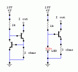
b) The current source built around R1, Q2 and Q3 is very inefficient (and not very good). As is, the power dissipation in the amp will be about 4 watts in R1 and about 2 to 2.5 watts each for Q1 and Q2. i.e. About half the power is wasted in R1. A more conventional CCS like those shown below would waste less heat. I'd vote for the 2 transistor one. BTW, the second one uses a LED as a zener. They make nice voltage references - low noise, low dynamic impedance etc, and pretty too.
c) ZTX450 is no good for the CCS, it's power dissipation is too low. Something like a BD139 would be better and can be mounted on a heatsink. See here for a list of other medium power transistors.
d) With single supply and large coupling caps, you need to beware of thumps at switch-on and switch-off. This can be a pain to sort out.
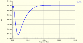
e) Don't forget to check power supply rejection. With mains power and ripple on the supply line, a fair amount of hum will leak into the signal path, mostly through Q1's bias resistor and the resistor feeding the CCS. It's a good idea to add an extra RC filter for these.
f) Heatsinks are rated according to their thermal resistance (in degrees centigrade per watt). e.g. If a transistor dissipating 2 watts is mounted on a heatsink rated at 10 degrees/watt, then the heatsink temperature will be 20 degrees higher than ambient. The transistor's case temperature will be a little higher due to the thermal resistance between case and heatsink, however this is low (maybe 1 degree/watt), so it won't make much difference here in a low power circuit.
Cheers - Godfrey
A couple of comments:
a) 1000uF for the input coupling cap (C1) is way to high. Something like 1uF would be better.
b) The current source built around R1, Q2 and Q3 is very inefficient (and not very good). As is, the power dissipation in the amp will be about 4 watts in R1 and about 2 to 2.5 watts each for Q1 and Q2. i.e. About half the power is wasted in R1. A more conventional CCS like those shown below would waste less heat. I'd vote for the 2 transistor one. BTW, the second one uses a LED as a zener. They make nice voltage references - low noise, low dynamic impedance etc, and pretty too.
c) ZTX450 is no good for the CCS, it's power dissipation is too low. Something like a BD139 would be better and can be mounted on a heatsink. See here for a list of other medium power transistors.
d) With single supply and large coupling caps, you need to beware of thumps at switch-on and switch-off. This can be a pain to sort out.
e) Don't forget to check power supply rejection. With mains power and ripple on the supply line, a fair amount of hum will leak into the signal path, mostly through Q1's bias resistor and the resistor feeding the CCS. It's a good idea to add an extra RC filter for these.
f) Heatsinks are rated according to their thermal resistance (in degrees centigrade per watt). e.g. If a transistor dissipating 2 watts is mounted on a heatsink rated at 10 degrees/watt, then the heatsink temperature will be 20 degrees higher than ambient. The transistor's case temperature will be a little higher due to the thermal resistance between case and heatsink, however this is low (maybe 1 degree/watt), so it won't make much difference here in a low power circuit.
Cheers - Godfrey
Attachments
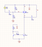
Turning the thing "upside down" with a positive-earth power supply can have some advantages:
a) Current drawn from the power supply is constant, so there's no signal current flowing in the power supply wiring. This can help with cross-talk.
b) Any ripple voltage on the power supply will not be applied to the Mosfet, which will help the PSRR, assuming the current source has good rejection and other PSRR issues are sorted out as well.
c) You can probably just short-circuit the output with a switch or relay during turn-on and turn-off to avoid thumps, without damaging anything.
p.s. I'm too lazy to draw all the other changes so pic below only shows the "upside down" configuration.
p.p.s. You need to add a gate-stopper resistor for the Mosfet to avoid oscillation.
Attachments
There are over 900 numbered posts in that thread, just the post number would help us find the diagram you are referring to.
900mA?
Why?
Headphones are over 100dB/mW, 1W would play over 130dB. Most phones are around 30R, so the bias need be no higher than about 250mA or so.
Sorry, that was a typo. I wanted to say 900mW. They each dissipate about a watt at loud listening levels, even more at max output. The mosfet is indeed biased to 300mA.
Godfrey: Thank you very much for the detailed analysis! I will try to incorporate all of your suggestions. The current mirror used here was what was taught in class, and I admit that I didn't do enough research on alternative current sources. The upside down amp is also a really neet idea.
Thanks again,
Chad
Sorry, that was a typo. I wanted to say 900mW. They each dissipate about a watt at loud listening levels, even more at max output. The mosfet is indeed biased to 300mA.
Nope, I am wrong again. Both transistors dissipate about a watt regardless of output... that is why its called a constant current source. I really have a lot to learn for this stuff.
So, in the CCS godfrey posted the transistor on the left is holding the emitter of the transistor on the right at ~.66 volt and R2 is responsible for the current reference. R2 dissipates less power because it is required to drop much less voltage than in my current mirror. Am I looking at this right, or is there something else going on? Is R1 just to bias the transistor on the right into active mode, and its value exact value relatively non-critical?
Thanks for all the help guys, I think this one project will teach me more than the entire semester of sitting in lecture!
Chad
Yup, you got it. 🙂So, in the CCS godfrey posted the transistor on the left is holding the emitter of the transistor on the right at ~.66 volt and R2 is responsible for the current reference. R2 dissipates less power because it is required to drop much less voltage than in my current mirror. Am I looking at this right, or is there something else going on? Is R1 just to bias the transistor on the right into active mode, and its value exact value relatively non-critical?
R1 provides base current for Q2 plus a few mA through Q1. It's often referred to as a "ring of two" current source here in the forum. Dunno the official name.
The nice thing about it is it doesn't just put a fixed voltage on Q2's base, but checks the actual current flowing through Q2. This defeats "Early effect", which is the slight change in Vbe when Vce changes.
😀I think this one project will teach me more than the entire semester of sitting in lecture!
Attachments

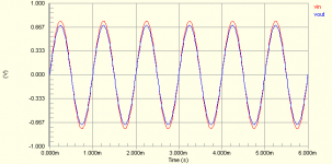
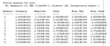
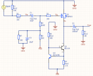
Ok. I have had some time to incorporate most of the modifications godfrey recommended. Right now my simulation uses an ideal power source and only has one channel modeled, so I haven't been able to quantify most of the desired effects. I did do a simulation of power supply ripple with the new bias filter circuit and it dramatically lowers hum. I don't think I understand how to implement a filter for the CCS. Each time I try to do it I actually make the hum larger then the output signal. Any ideas?
Any other improvements I can make that wouldn't dramatically overcomplicate the circuit?
Thanks!
Chad
Any other improvements I can make that wouldn't dramatically overcomplicate the circuit?
Thanks!
Chad
Attachments

Hi Chad
You can make it a bit simpler by removing R1 and increasing R5 to about 47K. That will also allow a much smaller value for C3.
To filter the CCS, you'd need to split R6 into two 470R resistors in series, and connect the mid-point to Vdd through a capacitor e.g. 100uF should give about -23dB @ 100Hz for that ripple source. I'm not sure if it's worth it, though - sim and see. What did you try before that made it that much worse?
On second thoughts, maybe it's a good idea to keep C3 quite large e.g. 100uF. Then the output voltage will take a few seconds to rise and fall at switch-on and switch-off. This should help to minimize thumps in the phones. The idea is to have the R4/R5/C3 time constant much larger than the C2/headphone time constant.
High impedance phones could still be a bitch, though. Maybe a 100 ohm resistor across the output (in parallel with the phones) would be a good idea to help with charging and discharging C2. This will help with high impedance phones and also avoid putting 7Vdc momentarily into the phones if the amp is switched on before the phones are plugged in.
Cheers - Godfrey
replace q3 with a To92 small signal device. High hFE and High fT.
The current through R6 should be between 50% and 10% of the current through R7, at present 11mA R6 and 270mA R7. If Vdd is -12Vdc then R6 can be between 89r and 430r.
Does Ibias need to be as high as 270mA? What is the maximum current that the headphones can survive?
Add 10r between Vs and C2. A charging resistor after C2, as suggested, would be a very good idea.
Replace C2 with a big polypropylene and then bypass it with an electrolytic to fill in the bottom couple of octaves.
I note that headphone is returned to Vdd. Was that deliberate? It allows the PSU to see a constant current load and thus very little variation in supply voltage as output power changes.
Last edited:
Is the 2n2222 a good choice? I really don't know how to go about finding good transistors, there are so many it seems impossible!replace q3 with a To92 small signal device. High hFE and High fT.
I currently have Vdd (should be Vss at this point I suppose) at -15V. The current I just decided on based on other designs I have seen on the internet. The amp does seem to linearize with larger current up until about 250mA, but the effect is not dramatic.The current through R6 should be between 50% and 10% of the current through R7, at present 11mA R6 and 270mA R7. If Vdd is -12Vdc then R6 can be between 89r and 430r.
Does Ibias need to be as high as 270mA? What is the maximum current that the headphones can survive?
The charging resistor makes perfect sense to me, but what would the resistor before C2 do?Add 10r between Vs and C2. A charging resistor after C2, as suggested, would be a very good idea.
I have seen this before, but is this just an audio standard practice? In physics we studied capacitors in some detail and it seems to me that if the plates of the large and small caps are held at the same potential their impedance would simply be summed. Perhaps the resistance in the wire allows for some amount of potential difference, but I am slightly skeptical. Is there a physical explanation for this phenomenon I am overlooking?Replace C2 with a big polypropylene and then bypass it with an electrolytic to fill in the bottom couple of octaves.
That was Godfrey's suggestion. He has been a great help so far with this project.I note that headphone is returned to Vdd. Was that deliberate? It allows the PSU to see a constant current load and thus very little variation in supply voltage as output power changes.
I think I am getting close to a functional design and I really appreciate everybody's feedback.
Chad
Vdd=-15Vdc is OK.
250mA from a single ended ClassA allows for enormous peak currents into worst case impedance headphones, or it allows for lot's of overhead at loud listening levels. The high overhead ensures that interference does not clip and that the normal signal is not clipped and is reproduced with only low levels of distortion.
But, will that 2r2 compromise the design and implementation of this amplifier?
I would be very tempted to use 10r for the CCS resistor. Leave the legs on the back of the PCB long to allow a second 10r to be added to give an effective 5r.
A third 10r and even a 4th, could be added (or removed) if you want to experiment with sound quality.
The peak output voltage from 15V supply will be about 7Vpk.
This is likely to be about the maximum that your headphone manufacturer specifies for non damaging signal peaks.
If we accept 5Vpk into 100ohm headphones and allow for the headphone drawing three times the expected current that a 100r resistor would demand, then maximum signal current will be about 3 * 5 / [100+10] <= 136mA.
If R6 passes 10% of that then R6 ~[15-1.2] / 0.014 ~ 1k0, if R7~5r.
Make R7 <<5r0 and R6 must be lower to meet that 10% to 50% condition.
2n2222 is 40Vce0, 600mA Id, >300MHz@20mA, hFE>75@10mA. Only the last, hFE, needs improving. Id could be relaxed substantially.
2n3904, 2n4401, bc336-16, bc546b, bc550c and a few of the MPSA series would all be suitable.
Last edited:
Hi AndrewDoes Ibias need to be as high as 270mA? What is the maximum current that the headphones can survive?
I think the issue here is low distortion rather than maximum output. With no global feedback deep class A seems like a good idea. At 1V rms output into 50 ohms, the current through the mosfet only varies about +-10% of it's quiescent value, which should give good linearity. The headroom is a bonus.
Hi ChadIs the 2n2222 a good choice? I really don't know how to go about finding good transistors, there are so many it seems impossible!
There's a very nice selection guide over here. I'd probably use the BC547B because it's cheap 'n cheerful (and familiar 🙂).
Cheers - Godfrey
....I think the issue here is low distortion rather than maximum output. With no global feedback deep class A seems like a good idea. At 1V rms output into 50 ohms, the current through the mosfet only varies about +-10% of it's quiescent value, which should give good linearity. The headroom is a bonus....
we are in complete agreement.............. or it allows for lot's of overhead at loud listening levels. The high overhead ensures that interference does not clip and that the normal signal is not clipped and is reproduced with only low levels of distortion...........
High overhead allows peak signals to pass without approaching peak power distortion.
So, I built this design and found some strange problems. First, the biasing resistor for the CCS (R6 in the new schematic) needed to be dramatically increased. Without a much larger resistor the current source did not work with |Vss|>10V. It caused a really strange distortion where just after the positive peak of a sine wave the output would dramatically distort with high frequency noise then settle back down before reaching 0V. Its hard to describe, and it took hours of playing around before I realized it was the CCS. Once I realized the CCS was to blame I tried to lower R6 thinking I needed more current, but that made it worse. It was not until I raised it all the way to 10K that everything straightened out. Why is this?
Next: It hums REALLY loud when the input is disconnected. With the input connected to a source it is as quiet as could be, but unplug the source and the hum is nearly as loud as normal listening levels.
Also, the sound quality is not exactly what I had hoped for. It is noticeably better than my macbook pro phones output, but not dramatically better. Using my 1st gen iPhone as a source the difference in sound quality is almost negligible. There is still a small difference, but not at all what I was expecting. Just for reference my iPhone has always sounded better with my Grados than the MBP.
Any ideas?
Attachments
- Status
- Not open for further replies.
- Home
- Amplifiers
- Solid State
- My First Amp