TOINO said:
quote:
Originally posted by Eva
… explain you the tricks to get low THD above 1Khz into 2 ohms (evil inductive coupling ) and to get the unity gain bandwidth product well past 1Mhz without having some of the output devices operating 180º out of phase with others at RF in a bucket-brigade fashion...
Please, go ahead.
That explanation would be very nice… I am “all ears” !
For what it is worth, I have used pretty much exactly the same PCB layout topology as described here for similarly (and higher) rated power output stages previously with complete success – in amplifiers which were actually completed and commissioned.
Strip line impedances are very low, as is inductive coupling due to reasons mentioned previously and phase shifts between the devices at the beginning and end of the chain don’t approach anything near 180 degrees out to HF.
I hope to have a complete 1kW class B amplifier operational in 3-4 weeks and I don’t expect the implementation to be any less successful this time round.
I’ll be posting the performance results here when it’s ready, of course.
Hartono said:hi Jacco,
their Hfe rating overlaps, still can find matched device, actually they're complementary so maybe no need to be matched.
some said complementary device matching is useless , I wonder if this is true when the device one side have 50 Hfe and another have 100
Hartono
DC Hfe, Hfe linearity and Hfe matching between complementary devices is one area in which the Sanken devices fall short.
The 2SC3264 has a nice fT of 60MHz, but it’s specified PNP complement is only 35MHz.
The MT-200 package is also a pain in real high power designs where lots of devices are required due to its nominal width of 36.4mm.
Indeed I am inquisitive about the EVA routing teachings, because I use the some layout as yours, except that I interleave the Pnp and Npn in the same row…with local decoupling on every transistor.
No problems so far.
Probably the optimal transistor distribution will be circular, with star output connection, but that is not always compatible with the standard hardware.
No problems so far.
Probably the optimal transistor distribution will be circular, with star output connection, but that is not always compatible with the standard hardware.
Remember that I'm in someone's ignore list and that SMPS PCB layout techniques are not appreciated here... 😉
Eva said:Remember that I'm in someone's ignore list and that SMPS PCB layout techniques are not appreciated here... 😉
Eva
Personally I -am- interested in your experience WRT high frequency
PCB layout applied to audio applications.
I think the tone of your posts was probably more resented than the
content.
Is it possible you can start another thread and discuss some issues
for the benefit of us all. I would imagine experience such that you
have is rather "thin on the ground" here.
cheers
Terry
High frequency PCB layout guidelines are somewhat complex and long to explain, but some basic hints are:
- Keep current loops small, tryng to carry complementary currents through opposite PCB layers so that the area of the resulting loop is just the thickness of the PCB multiplied by the length of the tracks.
- Place small signal circuits in a physical plane perpendicular to the power plane with the help of daughterboards. Use a ground plane with as little cuts as possible in both boards (it acts as a shorted turn near PCB leakage inductance).
- Treat power supply and speaker leads as inductors. Keep these leads together and the ones carrying complimentary currents twisted. Connect them to the PCB at the same point. Never sandwich the small signal section between the tracks of the supply rails (that's an ugly but usual practice).
- Use LC (or pi) filters to keep external RF (if any) stuff out of the PCB and to prevent the RF stuff generated in the PCB (class B switching or brief oscillations) from escaping through the wiring. Wiring is an evil thing.
- Class B output stages with many power transistors should follow a matrix structure (much in the same way as bipolar transistor dies are internally arranged). Interleaving NPN and PNP helps to get a magnetic flux more consistent with the audio signal out of the leakage inductances.
Now call me paranoid... (I don't mind)
"Interleaving NPN and PNP helps to get a magnetic flux more consistent with the audio signal out of the leakage inductances."
Is this useful for Class AB ? the music signal is asymetrical.
Is this useful for Class AB ? the music signal is asymetrical.
Also many Smps signals are asymmetrical.
Look at PFC or regulated Bridge. Indeed if you look to the signal on a scale near to “their period”, it seems chaotic as music. (Except the constant peak to peak)
In practice, if those smps are powering an amplifier, they are in fact modulated by music.
Look at PFC or regulated Bridge. Indeed if you look to the signal on a scale near to “their period”, it seems chaotic as music. (Except the constant peak to peak)
In practice, if those smps are powering an amplifier, they are in fact modulated by music.
Hartono said:"Interleaving NPN and PNP helps to get a magnetic flux more consistent with the audio signal out of the leakage inductances."
Is this useful for Class AB ? the music signal is asymetrical.
I don’t think so. Not so much due to the asymmetry of a typical audio signal, but the frequencies involved. Even the harmonic currents generated by the AB switching in even a reasonably fast slewing bipolar output stage aren’t that insidious, IMO.
The PCB I posted earlier could easily be modified for interleaved NPN/PNP devices in each row. Just run the complementary +/- power rails along the top and bottom of the PCB on opposite layers and run the pair of complementary “base lines” down each strip.
I honestly don’t see any real benefit from doing this though. In my experience, the best performance is had from linear bipolar output stages when the NPN/PNP devices and +/- rails are kept well separated from one another.
Cheers,
Glen
Eva said:High frequency PCB layout guidelines are somewhat complex and long to explain, but some basic hints are:
- Keep current loops small, tryng to carry complementary currents through opposite PCB layers so that the area of the resulting loop is just the thickness of the PCB multiplied by the length of the tracks.
- Place small signal circuits in a physical plane perpendicular to the power plane with the help of daughterboards. Use a ground plane with as little cuts as possible in both boards (it acts as a shorted turn near PCB leakage inductance).
- Treat power supply and speaker leads as inductors. Keep these leads together and the ones carrying complimentary currents twisted. Connect them to the PCB at the same point. Never sandwich the small signal section between the tracks of the supply rails (that's an ugly but usual practice).
- Use LC (or pi) filters to keep external RF (if any) stuff out of the PCB and to prevent the RF stuff generated in the PCB (class B switching or brief oscillations) from escaping through the wiring. Wiring is an evil thing.
- Class B output stages with many power transistors should follow a matrix structure (much in the same way as bipolar transistor dies are internally arranged). Interleaving NPN and PNP helps to get a magnetic flux more consistent with the audio signal out of the leakage inductances.
Now call me paranoid... (I don't mind)
Thanks Eva.
This all makes good sense. In a large design it would be difficult to achieve completely.
The proof of the pudding will be actual measurements of Glens
design especially at higher frequencies.
We will wait and see.
Terry
Terry Demol said:
Thanks Eva.
This all makes good sense. In a large design it would be difficult to achieve completely.
The proof of the pudding will be actual measurements of Glens
design especially at higher frequencies.
We will wait and see.
Terry
Besides the worth of the interleaving thing, there really isn't any other contention.
My last PA amp with the same output stage/layout topology did about 600W into 4ohms with about 0.01% THD at 20kHz. It was nothing special. Practically just a big D.Self “Blameless”.
Cheers,
Glen
I’m not sure to what extent I am doing anything productive here, as the technical details of my project I’ve posted so far have been, more than anything else, responsible for inciting patronising dismissals based on dodgy presumptions by some who obviously have never seriously designed and built anything similar, but here it goes anyway.
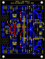
I’ve finished the Input and voltage amplifier stage PCB:
I’ve finished the Input and voltage amplifier stage PCB:
Attachments
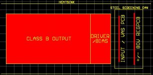
They say a picture says a thousand words, so here is one showing the physical layout, on a section of one of my big heatsinks as shown in this threads opening post, of a class B stage, using 3 of the modules described here already:
This is the section of the project I'm now proceeding to build and test first.
Cheerio,
Glen
This is the section of the project I'm now proceeding to build and test first.
Cheerio,
Glen
Attachments
Just wanted to say, Glen. Yer a fruitloop. Totally certifiable. This amp is so far beyond sensible it's just nuts. I'd love to hear it when it's done.
Oh, and I really hope you're on green power 😀
Oh, and I really hope you're on green power 😀
suzyj said:Just wanted to say, Glen. Yer a fruitloop. Totally certifiable. This amp is so far beyond sensible it's just nuts. I'd love to hear it when it's done.
Oh, and I really hope you're on green power 😀

So do you reckon doing a 5.1 channel surround sound set up would be out of the question?
Cheers,
Glen
PS
What do you think of the little HAM transmiter I picked up cheap?
http://users.picknowl.com.au/~glenk/CTM2K.HTM
G.Kleinschmidt said:I’m not sure to what extent I am doing anything productive here, as the technical details of my project I’ve posted so far have been, more than anything else, responsible for inciting patronising dismissals based on dodgy presumptions by some who obviously have never seriously designed and built anything similar, but here it goes anyway.
I’ve finished the Input and voltage amplifier stage PCB:
Of course it's productive 🙂
You're just working in a noisy environment.
G.Kleinschmidt said:…They say a picture says a thousand words…
Sceptic?...
If you go behind 1Kw you REALY need a good layout!..
At least on class-G, the switching peaks could only be controlled with the layout techniques that Eva talked about, and some more…
In the pictures you have one of my “Many-Kw-and-Kg-Interleaved-Transistor-Madness”

But I think that all this talk is a little threadjack.
Maybe the layout you use is good enough for your project.
I have only one layout question:
From where do you sense the feedback signal on your big output cooper area?
Attachments
- Status
- Not open for further replies.
- Home
- Amplifiers
- Solid State
- My 1024W RMS CLASS A+ amplifier.