Hi.
I got the MF-A1 for repair.
Someone had tried to repair the beast before and has done some strange stuff.
I have tried to replace all suspect parts.
One side of output transistors were dead.
So now after replacing and recapping, the amp doesn´t work.
I have about 400mV on the outputs and my output transistors don´t work and are not turned on.
Output transistors are healthy and all other transistors too.
Anybody have an idea?
looks like I am missing something but I can´t figure it out...
Thx.
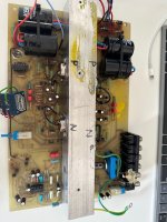
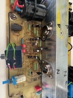
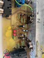


You would need to post the circuit as well. Voltage checks should reveal the issue but we need the circuit to begin 🙂
Hi.
Yes the supply voltage is about 25V on both sides (plus and minus).
here is the schematic.

THX.
Yes the supply voltage is about 25V on both sides (plus and minus).
here is the schematic.
THX.
I have about 400mV on the outputs and my output transistors don´t work and are not turned on.
Thanks for the circuit... you need to be precise in describing things 🙂
400mv on the outputs most would take to mean as no supply present. Do you mean you have a 400mv DC offset at the speaker output?
If you do mean that then 400mv is to high but not damagingly so for testing. Is there any audio present? i.e. does any channel work at all?
Are the -/+12 volt supplies OK (on the two Zeners)
Hi.
thank you for your comment.
i will try to be more precise.
i have about 400mV DC-offset, but the output transistors (MJ15003G and MJ15004G) stay cold, because they are turned off.
(amp is 20W class A and should run very hot...)
12V is also OK.
no sound due to not working output transistors...
I am very confused...
🤔
Have a close look at what you did. Both channels
affected in the same way hints at a supply problem.
"One side of output transistors were dead" - what
does it mean ?
affected in the same way hints at a supply problem.
"One side of output transistors were dead" - what
does it mean ?
THey were dead before I replaced it with newer ones MJ15003 and MJ15004.
I don´t know what kind of outputs were installed before... i threw them away.
yes i know that it must be a problem because both sides are the same.
but at the moment I am stuck in my brain with the problem...
I don´t know what kind of outputs were installed before... i threw them away.
yes i know that it must be a problem because both sides are the same.
but at the moment I am stuck in my brain with the problem...
Perhaps n and p are swapped.
Did you remove drivers, reinserted in the same way ?
You did not care to explain what "one side of output
transistors were dead" means - one channel, or else ?
Did you remove drivers, reinserted in the same way ?
You did not care to explain what "one side of output
transistors were dead" means - one channel, or else ?
hi.
yes the transistors should be correct.
before I did my recapping, one side of the outputs were blown.
I replaced both sides of the transistors...
yes the transistors should be correct.
before I did my recapping, one side of the outputs were blown.
I replaced both sides of the transistors...
For reference : never throw away any parts before repair is completely finished.
It is hard to destroy the final transistors, because this is a collector output.
"Should be correct" is not enough. Check that you did not rotate the heat sink bar.
It is hard to destroy the final transistors, because this is a collector output.
"Should be correct" is not enough. Check that you did not rotate the heat sink bar.
Hi.
The standard transitors were 2N3055/MJ2955.
I found that on the internet.
I replaced them with MJ15003G and MJ15004G.

this I found on the the homepage:

this is mine:

So i checked again and the transistors are in the right position.
The old transistors were checked with transistor tester and were definetly dead.
The standard transitors were 2N3055/MJ2955.
I found that on the internet.
I replaced them with MJ15003G and MJ15004G.
this I found on the the homepage:
this is mine:
So i checked again and the transistors are in the right position.
The old transistors were checked with transistor tester and were definetly dead.
Soldering wires directly to TO3 is bad practice. It also requires a soldering tool with above average power. These are sometimes not safe for semis.
I think you will have to measure the transistors and remount with solder lugs.
What is the situation with the parallel diodes? The PCB also seems DIY.
I think you will have to measure the transistors and remount with solder lugs.
What is the situation with the parallel diodes? The PCB also seems DIY.
i have about 400mV DC-offset, but the output transistors (MJ15003G and MJ15004G) stay cold, because they are turned off.
I'll have a closer look later but the 400mv offset is puzzling because it points to no gross failure anywhere. Its not the most intuitive of circuits but it splits neatly into a top and bottom half with one mirroring the other.
(have you checked the 0.22 ohm resistors are OK and which actually seem to be 0.47 ohm in your picture?)
You must carefully check voltages including checking across base/emitter junctions to see if devices are trying to be turned on. Output TR10 and driver TR8 should try and turn fully on via R10. The PNP output and driver should be doing the same.
TR5 and TR7 provide the means for reigning in the massive current that should be flowing.
Its odd because a fault on one half or the other would be expected to give a high offset and that obviously isn't happening.
Checked a few times. everything insulated as it should be!Check insulation of collectors to the bar and correct soldering of base/emitters.
hi.Soldering wires directly to TO3 is bad practice. It also requires a soldering tool with above average power. These are sometimes not safe for semis.
I think you will have to measure the transistors and remount with solder lugs.
What is the situation with the parallel diodes? The PCB also seems DIY.
this is the original design of Musical Fielity.
The Collector was soldered directly to the PCB.
The PCB is one of the first A1 made. This is definetly a original PCB from Musical fidelity.
😉
Output devices are measuring OK. They are still alive!
😀
The paralleled diodes are shown in the shematic and are OK .
see picture:
Paravicini invented this practice.Soldering wires directly to TO3 is bad practice.
yes, rechecked now...Sure that base and emitter are not swapped ?
- Home
- Amplifiers
- Solid State
- Musical Fidelity A1 - Problem