Papa has published so many variants of SIT amplifiers. A question will always pop up, which one sounds better or which one I should build. The standard answer will always be: you need to try them all, or it is worth to building them all.
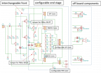
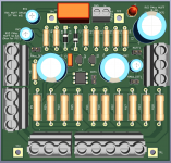
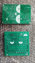
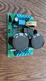
The multi configurable Testing PCB is trying to satisfy them all.
I wish your experienced DIYER can chime in and we can make it better. At end of it, I will order PCB and test build it. All design files for it will be public here and everyone can use.
Configurable end stage
AMP1, SIT N-Mosfet MUFF, close Jumper for NMos MUFF, open Jumper for PMos MUFF, jump and short all pins PMOS Conn
AMP2, SIT P-Mosfet MUFF, open Jumper for NMos MUFF, close Jumper for PMos MUFF, jump and short all pins NMOS Conn
AMP3, SIT P-Mosfet DEFiSIT, close Jumper for NMos MUFF, close Jumper for PMos MUFF, jump Pin1 and 3 of NMOS Conn, bridge SIT Conn Pin 2 and NMos Pin2
Configurable power
V+ and GND: V+ on Pin3 of Configurable PW Conn, jump Pin2 and Pin1 as GND
V- and GND: V- on Pin1 of Configurable PW Conn, jump Pin2 and Pin3 as GND
V+/- and GND: connect as shown
Speaker connector, you can try different Rs and Rm for different THD and 2nd and 3rd ratio
Interchangeable front end
The famous Fjet buffer is designed in. four connecting points are designed, V+, V-, Output and GND. Using bronze spacers. A daughter board can be build up and add-on. If not needed, just not put Jfets on, then your external drive board can be used.
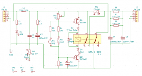
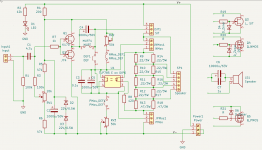
The final power board schematics for 48V SMPS is in the post #19.
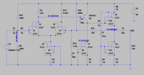
The final amplifier schematics is in the post #20.
The measurement started from the post #33.
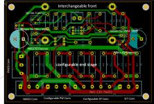
The zipped KiCad projects for the amp and power are in the post #36, feel free to use them.
The +/-24VDC power supply with Mean Well DC-DC module is added in the post #41
The FE with IC headphone amp + Edcor transformer is added in the post #43
The FFT measurements for output power at 1, 5 , 10, 15, 20 W are added in #44/#45
The SIT amp sounds super with Pass BA-3 FE. You guys need to try it!
A Salas DCG3 front end and DCSTB power reg were built to drive the SIT amp. This is my 3rd FE in the testing in #50.
If I am not mistaking, the build is the first DIY of Papa's SIT MUFF with N-Mosfet. As Pa said, big N-Mosfet is easier to get and have more choices. And they are more consistently built than P-Mosfet, based on my very limited 4 samples testing.
The sound of the amp is the best so far in my DIY experiences. I will listen it for long. So I won't test the PCBs boards for other builds in short time.
After I built F4, DefiSit, Lufet and SIT MUFF and listen all of these passive follower without gain, I have an impression(Maybe I am wrong). They sound little bit too lazy. Like a very passive dancing partner, it needs a very active, vivid and forceful front end to drive it and bring it to life.
I hope the upcoming Pa's front end can bring it.
The multi configurable Testing PCB is trying to satisfy them all.
I wish your experienced DIYER can chime in and we can make it better. At end of it, I will order PCB and test build it. All design files for it will be public here and everyone can use.
Configurable end stage
AMP1, SIT N-Mosfet MUFF, close Jumper for NMos MUFF, open Jumper for PMos MUFF, jump and short all pins PMOS Conn
AMP2, SIT P-Mosfet MUFF, open Jumper for NMos MUFF, close Jumper for PMos MUFF, jump and short all pins NMOS Conn
AMP3, SIT P-Mosfet DEFiSIT, close Jumper for NMos MUFF, close Jumper for PMos MUFF, jump Pin1 and 3 of NMOS Conn, bridge SIT Conn Pin 2 and NMos Pin2
Configurable power
V+ and GND: V+ on Pin3 of Configurable PW Conn, jump Pin2 and Pin1 as GND
V- and GND: V- on Pin1 of Configurable PW Conn, jump Pin2 and Pin3 as GND
V+/- and GND: connect as shown
Speaker connector, you can try different Rs and Rm for different THD and 2nd and 3rd ratio
Interchangeable front end
The famous Fjet buffer is designed in. four connecting points are designed, V+, V-, Output and GND. Using bronze spacers. A daughter board can be build up and add-on. If not needed, just not put Jfets on, then your external drive board can be used.
The final power board schematics for 48V SMPS is in the post #19.
The final amplifier schematics is in the post #20.
The measurement started from the post #33.
The zipped KiCad projects for the amp and power are in the post #36, feel free to use them.
The +/-24VDC power supply with Mean Well DC-DC module is added in the post #41
The FE with IC headphone amp + Edcor transformer is added in the post #43
The FFT measurements for output power at 1, 5 , 10, 15, 20 W are added in #44/#45
The SIT amp sounds super with Pass BA-3 FE. You guys need to try it!
A Salas DCG3 front end and DCSTB power reg were built to drive the SIT amp. This is my 3rd FE in the testing in #50.
If I am not mistaking, the build is the first DIY of Papa's SIT MUFF with N-Mosfet. As Pa said, big N-Mosfet is easier to get and have more choices. And they are more consistently built than P-Mosfet, based on my very limited 4 samples testing.
The sound of the amp is the best so far in my DIY experiences. I will listen it for long. So I won't test the PCBs boards for other builds in short time.
After I built F4, DefiSit, Lufet and SIT MUFF and listen all of these passive follower without gain, I have an impression(Maybe I am wrong). They sound little bit too lazy. Like a very passive dancing partner, it needs a very active, vivid and forceful front end to drive it and bring it to life.
I hope the upcoming Pa's front end can bring it.
Attachments
Last edited:

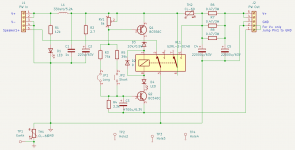
Mean Well power brick as used in Papa’s V-fet amp is to be used. The first stage is copied from Mark Johnson’s published HF filter for Mean Well. The middle stage is Papa’s new slow on/ fast off circuit. I still like big Capacitors more than regulator, so I put C-R-C filter behind them. To prevent Inrush current to shut off SMPS when turn on with big Caps, a CL-60 is put between. It will be short at the same time when speaker is in use.
Attachments

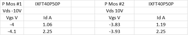
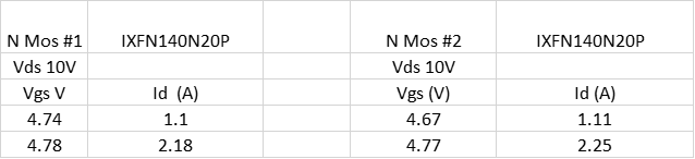
while waiting for the PCBs, bought two IXFN140N20P and two IXTN40P50P, made few tests. 2 N-Mosfets are pretty close and 2 P-Mosfets are far apart.
The strange thing is that N-Mosfet Id-Vds-Vgs curve looks very not Mosfet in very low Vgs.
The strange thing is that N-Mosfet Id-Vds-Vgs curve looks very not Mosfet in very low Vgs.
Attachments
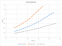
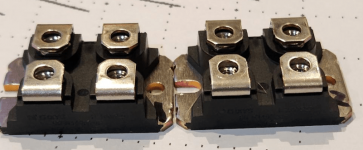
I always measure parts from high to low. That means highest voltage and current point was set at first, waited for the readings getting stable, then started next lower point. It may be caused by the tempco. But I couldn't find any measurement in the area in which we are use these big guns.
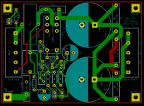
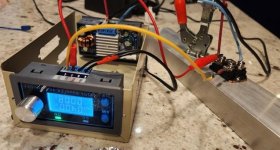
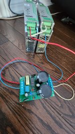
The PW board were assembled. They were tested using two 24V SMPS as 48VDC. One bug was found on PCB and corrected. The on-delay at very light load is 6 seconds. Turning off is quick when the voltage drops to around 46V.
Attachments
- Home
- Amplifiers
- Pass Labs
- Multi Configurable Testing PCB for Papa’s SIT-PMosfet, SIT-NMosfet MUFF and DEFiSIT Amplifier