Hi Donpetru!formula 22,
That diagram audio amplifier seems not optimized. For example, there is no point can mount only trim P1 in the input circuit of the audio amplifier. Right is to mount a resistor in series with the trim P1. But so, not 100% good. It's much better to try to let the resistance instead of P1, but that only after having established experimental optimum value of current in the input circuit. Bootstrap capacitor C8 is no current solution. It's old-fashioned, as is diagram audio amplifier. Then, R2 and R9 are too high.
Finally, if you want one audio amplifier diagram worth done, download and analyze all schematics (pdf files) that were posted in this topic or thread:
KIT 0205 - schema, modernizare, constructie amplificator - Comunitatea Tehnium Azi
Nice day.

Is enough for R2 and R9 to put 27k (about 30dB gain) or go to 22k?
If you replace the resistors (R2 and R9) that further changes are needed in the shematic?
For P1 to put a fixed resistor with 750 ohms or some other value?
Thank you for your cooperation!
Last edited:
1) R2 = R9 = 22K is an optimal value. This value is chosen according to the defining characteristics of the input transistor amplifier (more precisely, according of the hFE transistors T1 and T2 from the schedule attached to you before). If you change these resistors you will have to decrease the value of R6 (for example, R6 = 510 ohm).
2) Trim P1 can be replaced with a resistor of 560 Ohm. This value resistor will lead to getting the best performance with minimal power dissipation on T1 and T2. Then, by choosing that value, voltage drop resistors R4 and R4' not exceeding the maximum allowed. It's very important that, because resistance values R4 and R4' and quality of these resistors, greatly influences the SNR input amplifier and even the entire SNR audio amplifier.
2) Trim P1 can be replaced with a resistor of 560 Ohm. This value resistor will lead to getting the best performance with minimal power dissipation on T1 and T2. Then, by choosing that value, voltage drop resistors R4 and R4' not exceeding the maximum allowed. It's very important that, because resistance values R4 and R4' and quality of these resistors, greatly influences the SNR input amplifier and even the entire SNR audio amplifier.
Mr. Donpetru, the resistor P1 I put the 750ohm, and resistors R4 and R4 'set of 100R trimmer. For the transistors T1 and T3 have set BC560C amplifier works well. With the DC-offset at the output amplifier is approximately + /-5mV.1) R2 = R9 = 22K is an optimal value. This value is chosen according to the defining characteristics of the input transistor amplifier (more precisely, according of the hFE transistors T1 and T2 from the schedule attached to you before). If you change these resistors you will have to decrease the value of R6 (for example, R6 = 510 ohm).
2) Trim P1 can be replaced with a resistor of 560R. This value resistor will lead to getting the best performance with minimal power dissipation on T1 and T2. Then, by choosing that value, voltage drop resistors R4 and R4' not exceeding the maximum allowed. It's very important that, because resistance values R4 and R4' and quality of these resistors, greatly influences the SNR input amplifier and even the entire SNR audio amplifier.
Do I reduce resistor P1 = 750R on 560R the BC560C transistors with this?
thanks and cheers!

Last edited:
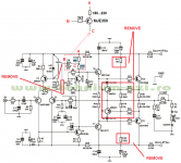
Hi Donpetru!
Is should look like this schematic amplifiers?
What circuit protection from excessive current
recommend?
Thanks and cheers!
Is should look like this schematic amplifiers?
What circuit protection from excessive current
recommend?
Thanks and cheers!
Attachments
Last edited:
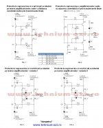
See pictures below:
FIG.1 - Overload and short circuit protection the output audio amplifier with the limit average current through the output transistors.
FIG.2 - Overload and short circuit protection the output amplifier bringing back to zero current output transistors.
FIG.3 - Overload and short circuit protection the output amplifiers - version I
FIG.4 - Overload and short circuit protection the output amplifiers - version II
I recommend Fig.3.
When using schematic figure 2 (or FIG.2), between points 1 and M, 2 and N, are mounted each one resistor.
Attachments
I pray for the values of components for round the Fig. 3, for my schematic.See pictures below:
FIG.1 - Overload and short circuit protection the output audio amplifier with the limit average current through the output transistors.
FIG.2 - Overload and short circuit protection the output amplifier bringing back to zero current output transistors.
FIG.3 - Overload and short circuit protection the output amplifiers - version I
FIG.4 - Overload and short circuit protection the output amplifiers - version II
I recommend Fig.3.
When using schematic figure 2 (or FIG.2), between points 1 and M, 2 and N, are mounted each one resistor.
thank you !
Many mosfet power amplifiers based on 2SJ162/2SK1058 lateral mosfets are made. This one is particularly suitable for home-use, being small, having moderate power with very low distortion:
Available as complete kit or pcb-only, so you can select components yourself. Mosfets/components are also available separately.
- Max output power: 100W@8ohm, 150W@4ohm
- THD+N (1kHz): < 0.005% (measured!)
- PCB dimensions: 100x60mm
- Input sensitivity: 1.2V rms
- Input impedance: 22kohm
- Bandwidth: 80kHz
- Voltage gain: 27dB
More info:
Mosfet Power Amplifier
dear sir can you send me this pcb design on my e mail i,ll be highly obliged.thanking you
- Status
- Not open for further replies.
- Home
- Vendor's Bazaar
- Mosfet power amplifier 2SJ162/2SK1058