To run my LM4702 amplifier "inverted" I need to outboard a couple opamps, (probably the OPA2604 which will run off +/- 24V rails.) Ergo hoc, i did some research on the 2-Transistor Regulator from Morgan Jones "Valve Amplifiers, 4th ed."
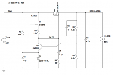
Here's the adapted schematic -- using the 2SB649AC and 2SD669AC which i have in abundance. The reference is a 9.1V zener:
Note that the output cap is now 4.7uF rather than 47uF in the book. The latter seems to overdamp the regulator:
Here's the adapted schematic -- using the 2SB649AC and 2SD669AC which i have in abundance. The reference is a 9.1V zener:
An externally hosted image should be here but it was not working when we last tested it.
Note that the output cap is now 4.7uF rather than 47uF in the book. The latter seems to overdamp the regulator:
An externally hosted image should be here but it was not working when we last tested it.
Thanks for showing this! I'm a little surprised there isn't a pole-splitting compensation capacitor in the error amplifier, but perhaps that's merely personal taste or prejudice. If you are happy with the transient response to an output current step (say from 2% max load, to 100% max load) then you're happy.
There seems to be 51 volts across R5, so it dissipates 460 mW. Maybe splitting it into two 2.7Ks in series, would let you use lower wattage resistors. It would also provide an intermediate node where another bypass capacitor could possibly go.
If the overriding goal is to minimize transistor count then it's easy to see why Q3's collector load is a resistor. But if it's acceptable to add another semiconductor device, replacing R6 with a current source might be a good idea. It'd increase the voltage gain of the error amplifier, reducing output impedance of the closed loop voltage regulator. And with 40 volts (!!!) across it, there is plenty of headroom to implement pretty much any 1-device current source ever invented. I'd probably favor a PNP with a 5K emitter degeneration resistor for incredibly high output impedance. At 3 mA of bias current it would drop 15 volts across the emitter resistor, which is unusually high. Hey you've got 40 volts to play with; put em to good use. I bet the resulting high gain error amplifier would need explicit frequency compensation, pole-splitting or otherwise.
Best regards, MJ
Here's what I mean.
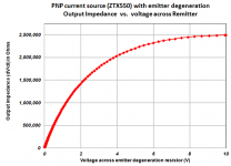
I simulated a 3 milliamp current source using a PNP with emitter resistor Re, and measured the output impedance of the current source as a function of (the voltage dropped across the emitter resistor).
Current was a constant 3.0 mA in each case.
I exported the results to Excel and made a plot, attached below. More voltage dropped across the emitter resistor, gives greater output impedance - with diminishing returns. In the Morgan Jones voltage regulator, the gain of the error amplifier is approx (gm_q3 x Zload). Installing this PNP current source in place of R6 would raise Zload from 12K to about 2Meg, increasing gain pretty substantially. Assuming of course that Zin(U2) is not a significant factor.
Attachments

And the LM317L is incredibly cheap. Avnet Express (a qualified TI distributor who stocks genuine, factory direct, non-counterfeit parts) sells it for $0.04 in quantity one: {LINK} . Stock=1591, can ship immediately.
The LM317L's datasheet min output current is 2.5 mA, and in this application you're running 3 mA, so no problem there.
Its max (Vin - Vout) voltage delta is 35 volts, and in this application you're running 40 volts. So you'll probably want to add a new series element in that circuit branch, to drop some of the voltage. Maybe a 4.7K resistor? Maybe another 9.1V zener diode? This introduces a new circuit node and thus, a new spot to contemplate installing a new bypass capacitor for additional noise reduction.
I tried the LND150 -- not enough go-juice. The DN2540 is a bit big for this application. Simulating the LM317L it looks like we pick up 12 to 15dB of gain.
This is a WOW -- thanks for the recommendation -- Negative Regulator with LM337 with 1K between ADJ and OUT = 1.2mA -- (the 12K resistor was doing about 0.8mA)
An externally hosted image should be here but it was not working when we last tested it.
Hm, node 5 (output) = -20.5 volts
Thus node 2 = -19.8 volts since V(2) = V(5) + VBE(U1)
Node 3 = Vin = -60V
Thus the voltage across R2 is V(2,3) = 40 volts
So the current in R2 is 40/12k = 3.3 mA
I'd be a little concerned about running an LM337 at just 1 mA since the datasheet commands you to run more.
Now that the error amplifier has a current source load, loop gain is limited by the input impedance of the series pass transistor (emitter follower). You could raise this impedance by using either a darlington EF or a complementary feedback pair (Sziklai) EF **. However it does add one more active device.
** Or by using a MOSFET for the series pass element!
Attachments
Graph above is with a TIP147 -- the error amp can't source enough current to the normal pass device. I am running 50mA which should be Ok for the buffer, inverter and servo. Higher current means lower output impedance.
Actual current from the LM337/317 in this mode is about 1.5mA. I'm not worried about running it at less than the recommended amount -- as it appears to be pretty stable.
Your observation about the max voltage across it -- there's about 12.5V across the Zetex, 9.1 on the Zener and the rest across the current source -- so I am just putting two in series!
Tried a diode buffered JFET current source (figure 9C in Jung's article "Current Sources") and it wasn't much better than the LM337/317 in this application.
Here's what happens when the series pass element becomes MOS; now the error amplifier's dc gain achieves its maximum possible value, (gm x ro), which is about 1000X or 60 dB.
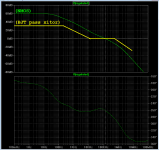
I was in a hurry so I just installed a simplistic lag-lead compensation; phase margin at unity gain crossover is about 95 degrees. You could play with this some more if you wished.
New circuit's Bode plot in green; my hamfisted attempt to draw a copy of the previous circuit's Bode plot, in yellow.
I was in a hurry so I just installed a simplistic lag-lead compensation; phase margin at unity gain crossover is about 95 degrees. You could play with this some more if you wished.
New circuit's Bode plot in green; my hamfisted attempt to draw a copy of the previous circuit's Bode plot, in yellow.
Attachments
Here's a simulated comparison of the 2-Transistor with an NMOS pass device and the Darlington:
An externally hosted image should be here but it was not working when we last tested it.
Looks like the Darlington-ness of the TIP142 is giving you a Zin sufficiently high that it doesn't degrade the low frequency gain of the error amplifier. But I would have thought that a MOSFET has an even higher Zin, thus an even higher gain at dc. Oh well, faulty intuition. Again. The TIP is probably cheaper and probably needs fewer protective components; easy decision.
Edit- apologies for an error in the Bode plot I posted. The yellow line is your first circuit with no current source. I copied from the wrong post! sorry, MJ
Edit- apologies for an error in the Bode plot I posted. The yellow line is your first circuit with no current source. I copied from the wrong post! sorry, MJ
Last edited:
The LM317L is voltage limited, so are the JFETs (40V max) -- will probably go to a DN2540N3 -- the TO-92 package.
- Status
- Not open for further replies.
- Home
- Amplifiers
- Power Supplies
- Morgan Jones 2 Transistor Regulator