Bernhard said:Both inputs tied together to source: Silence.
By "tied together to source", did you mean that literally? That is, are both the + and - input shorted together at the signal source?
Or is it a balanced output source?
Erik
That is, are both the + and - input shorted together at the signal source?
Yes, which means that common signals are rejected.
At this point I would recommend that you consider a current-feedback type op amp with a booster stage similar to what we've been looking at for ordinary op amps.
While I still think the arrangement with ordinary (voltage input) op amps can be made to work, it's apparent that at best it requires actively driven balanced inputs.
While I still think the arrangement with ordinary (voltage input) op amps can be made to work, it's apparent that at best it requires actively driven balanced inputs.
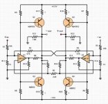
OK, I worked up a probable schematic, which you can find at www.passlabs.com/temp/YAX2.tif in a compressed tiff format.
In this schematic we are using two "current feedback" op amps much in the same manner as we began in this thread, but with current boosters as later described.
R0 is the "magic" resistor which creates the SuperSymmetric connection. R9/R10 and R11/R12 are low impedance voltage dividers so the outputs will swing voltages higher than the op amps output.
R15 and R16 can be used for absolute DC stabilization, as are R13 and R14. The gain should be R2/R1.
R2=R4, R9=R11, R10=R12, and so on.
This circuit has not been tested or simulated, only envisioned.
Nelson Pass said:
In this schematic we are using two "current feedback" op amps much in the same manner as we began in this thread, but with current boosters as later described.
Thanks Nelson, this might give us a new boost.
Until now JH and I were using the inverted input of the opamps.
In your new drawing, the uninverted is used, and R2/5 are tied together, R4/7 not. I assume R4/7 is correct.
Another problem I encountered was the dividing of R0 into two halves and connect the centerpoint to ground to make things work.
http://www.diyaudio.com/forums/showthread.php?postid=143661#post143661
/Hugo
questions:
how much power can the amp deliver and what would be the best bias current per output device ?
will the amp sound better / will this be audible if it is "X" and will the sound be better than that of an aleph ?
How strong has to be the transformer ?
how much power can the amp deliver and what would be the best bias current per output device ?
will the amp sound better / will this be audible if it is "X" and will the sound be better than that of an aleph ?
How strong has to be the transformer ?
should not!
mlloyd1
mlloyd1
grataku said:Nelson,
I think there is a mistake in the schematic...should R2 be connected to R5?
According to my experiments with VFB op amps, it seems that the op amp outputs must be directly associated with their inputs in a way or another.
After all, to go with YAX2 this time, I ordered CFB op amp, LM6181. I expect the delivery in 10 days. Attached below is the circuit of YAX2 of Nelson Pass, with additional emitter resistors and the output-to-ground resistors. This is made mainly for a better communication.
JH
After all, to go with YAX2 this time, I ordered CFB op amp, LM6181. I expect the delivery in 10 days. Attached below is the circuit of YAX2 of Nelson Pass, with additional emitter resistors and the output-to-ground resistors. This is made mainly for a better communication.
JH
Attachments
jh6,
Although it seems to be a very fashinating circuit with potential to make all bjt lovers happy, I can't get past the fact that it contains opamps so I can't get into it.
Although it seems to be a very fashinating circuit with potential to make all bjt lovers happy, I can't get past the fact that it contains opamps so I can't get into it.
jh6you said:This is made mainly for a better communication.
JH
Thanks JH,
Any idea of values of several resistors?
I've been trying to make this circuit work on the sim, without any result.
For R5 to R7 I took the classical 100-200ohm values. (With MJ15030/31.
But no way to find out what values to put at R19/10/11/12/15/16.
Looks like you also have no clue?
Here in Belgium, Farnell delivers in one day.
Strange, it will take ten days for your 6181; As Leocom is a daughter of Farnell?
/Hugo
grataku said:I can't get past the fact that it contains opamps so I can't get into it.
As Nelson stated in his first post: "Or build something discretely......" 😉
/Hugo
Netlist said:
Any idea of values of several resistors?
I would like to think about--with time.
The delivery could be in 2-10 days--just guessing.
You must know that I am very eager to get it right away! 😉
JH
jh6you said:
You must know that I am very eager to get it right away! 😉
JH
Whish I could Mail or Fax them to you...
/Hugo
grataku said:
very fashinating circuit with potential
Yes, it is. I always like to experience new fashionating thing.
To me, young mind is very important. 🙂
JH
JH,
This looks exactly like my design in post 252 except addition of R0 between the two inverting inputs of the OPs. 😉
I believe R9 R10 R12 R12 R13 R14 are not essential for function, but make the circuit more difficult to survey.
Also I wonder if R0 is necessary because ( the hides in the detail ) the connection between the two inverting inputs of the OPs is already made by the load.
But I could miss something...
May be Nelson likes to give his statement.
According to my experiments with VFB op amps, it seems that the op amp outputs must be directly associated with their inputs in a way or another.
This looks exactly like my design in post 252 except addition of R0 between the two inverting inputs of the OPs. 😉
I believe R9 R10 R12 R12 R13 R14 are not essential for function, but make the circuit more difficult to survey.
Also I wonder if R0 is necessary because ( the
hides in the detail ) the connection between the two inverting inputs of the OPs is already made by the load.But I could miss something...
May be Nelson likes to give his statement.
And now - what ? 
I could solder in that R0 and plug in that LM6181.
If the circuit does not work anymore with this modification, I will know that was the wrong direction.
But if it still works, how to know wether it is supersymmetric or not, and how to know wether it was supersymmetric or not before ? 🙁
🙁 
I could solder in that R0 and plug in that LM6181.
If the circuit does not work anymore with this modification, I will know that was the wrong direction.
But if it still works, how to know wether it is supersymmetric or not, and how to know wether it was supersymmetric or not before ?
🙁 What we need is some kind of SOI * 😎
* Supersymmetric Operation Indicator = a light, that flashes when supersymmetric operation of a circuit occurs.
* Supersymmetric Operation Indicator = a light, that flashes when supersymmetric operation of a circuit occurs.
Bernhard said:What we need is some kind of SOI * 😎
* Supersymmetric Operation Indicator = a light, that flashes when supersymmetric operation of a circuit occurs.
Make it a SOIL: Replace the "magic" resistor with a lamp or LED
The problem will be, which lamp.
Definitely take a blue one!

The main difference between your and Nelson's circuit indeed is R0 and the way you connect the inverted inputs.
BTW, got some results on the sim.
Can you tell us some more how you found your resistor values?
Or was it also "by accident"? 😉
/Hugo
- Status
- Not open for further replies.
- Home
- Amplifiers
- Pass Labs
- Monolithic SuperSymmetry with Current Feedback