that is, you don’t understand how the output stage is turned on?It is not Darlington, strictly speaking it is emitter follower.
You can always look at the attachment.
AND?I quete what you write "You do not have the appropriate education"
In electronics, a multi-transistor configuration called the Darlington configuration (commonly called as a Darlington pair) is a circuit consisting of two bipolar transistors with the emitter of one transistor connected to the base of the other, such that the current amplified by the first transistor is amplified further by the second one.[1] The collectors of both transistors are connected together. This configuration has a much higher current gain than each transistor taken separately. It acts like and is often packaged as a single transistor. It was invented in 1953 by Sidney Darlington.
Gennady's output stage is assembled according to the Loccanti scheme. In which the driver transistors operate in Class A . Sincerely StanislavIn electronics, a multi-transistor configuration called the Darlington configuration (commonly called as a Darlington pair) is a circuit consisting of two bipolar transistors with the emitter of one transistor connected to the base of the other, such that the current amplified by the first transistor is amplified further by the second one.[1] The collectors of both transistors are connected together. This configuration has a much higher current gain than each transistor taken separately. It acts like and is often packaged as a single transistor. It was invented in 1953 by Sidney Darlington.
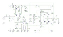
That's right, this stage was the first modification made to the amplifier board from the first post. If you compare both the diagram on a piece of paper and the screenshot of the model.Gennady's output stage is assembled according to the Loccanti scheme. In which the driver transistors operate in Class A . Sincerely Stanislav
"Darlington" was written as a common noun, but the translator writes it as Darlington.
- Input progressive equalization filter for amplifier stability is described in a scientific article
- the possibility of multi-pole correction in the negative feedback circuit is based on the calculated control of the occurrence of positive feedback. Its advantage is only in the number of zeros after the decimal point for distortion estimates. There is an example in this topic - when an output stage in class B was able to reduce distortion in the model by 30 times without increasing the linearity of the input stage - this is nonsense from a practical point of view. The same is true for multi-pole correction in the negative feedback circuit.
- The sound assessment in tests is based on the quality of the input stage; multi-pole correction does not cover it and has virtually no effect on the average sound assessment.
Last edited:
I think you should post your latest schematic of this interesting amplifier here.
That can make us get back on track in this topic.
That can make us get back on track in this topic.
no problem, see attachmentI think you should post your latest schematic of this interesting amplifier here.
That can make us get back on track in this topic.
I also added the original version (on a piece of paper) according to which this version of the amplifier was made.
modifications:
1. the middle point of the pre-output repeater resistors was disconnected from the common output - this reduced distortion by 4 times
2. progressive compensation has been introduced - this is the input filter R1/R4C2 and the load circuit output to the voltage amplifier R24C8 - these two circuits are included as coefficients of the equation of state variables, because when increasing the linearity of the input stage, it is necessary to limit the input spectrum (using a progressive filter) without a significant change in phase - this is the only way it works and these concepts should not be separated, because this contradicts the meaning of this progressive compensation.
The purpose of the correction (progressive compensation) is to increase the linearity of the input stages, which determine the sound quality of the amplifier
3. It is planned to re-solder VT5VT6 (circuit on a piece of paper) as Q3 Q8 - this will stabilize the operation of the input differential stages at large signal values at the input of the circuit, which will reduce distortion more in 3 times.
P.S. Post No. 12 shows how an output stage in class B was able to reduce distortion by 30 times without changing the compensation circuits - this is modeling nonsense, and has nothing to do with the actual sound, so this option is not considered, but in the model everything looks good in terms of distortion.
Attachments
Last edited:
Enough. Fourteen posts have been deleted in an attempt to clean this this mess up. Personal insults have no place here.

(Below) attachment is just a "leach" with NO compensation ? Unless you count C10/11 as comp. ?
It might not outright oscillate , but would "ring" like hell.
"Varient" has C8/R24 , "shunt" ? .... 2X small miller caps at VAS cb work better.
Edit - I suppose an EF2 can be a darlington. Why not go all the way - EF3 or even a Lateral OPS ?
OS
It might not outright oscillate , but would "ring" like hell.
"Varient" has C8/R24 , "shunt" ? .... 2X small miller caps at VAS cb work better.
Edit - I suppose an EF2 can be a darlington. Why not go all the way - EF3 or even a Lateral OPS ?
OS
Attachments

Are you able to provide a reference for this scientific article Hennady? I would be interested to read it. Thanks.That's right, this stage was the first modification made to the amplifier board from the first post. If you compare both the diagram on a piece of paper and the screenshot of the model.
- Input progressive equalization filter for amplifier stability is described in a scientific article
The diagram on sheet C10/C11 shows the wrong connection.Unless you count C10/11 as comp. ?
In fact, on the board they connect the base and collector VT10/VT11, just such an implementation can be called a shunt. This is not a very good solution, since stability will depend on the gain and the higher the gain, the higher the stability. The second point is that on the leaflet the output stage is switched on by Dalington, and to control the base currents at hight frequencies, less resistance of the voltage amplifier is needed. The inflection point of the frequency response will depend on the parameters of the elements and temperature. This probably won't be very good for the sound.
That is why Darlington was separated into two stages in which the first stage of emitter follower in class A mode.
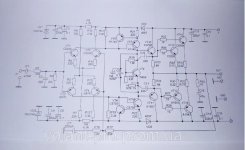
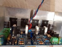
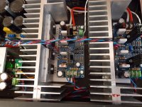
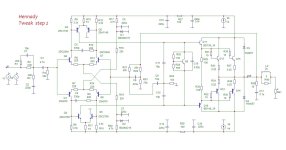
1 step of tweaking the amplifier was made according to the diagram on the piece of paper https://www.diyaudio.com/community/attachments/shema-for-mod-henk-jpg.1275208/.
The Tweak diagram is in the attachment, with red frames around the elements that were changed on the board and added to the back of the circuit board. Photos of the process are also attached.
Managed to get a very clean and comfortable sound, but we can do better, but only by changing the topology. The reason for the shortcoming in this topology is the unsatisfactory operation of the input differential stage loaded on the voltage amplifier (2nd stage) - it is difficult to control distortion. Using progressive compensation, we managed to distort them by a factor of 2 at a frequency of 20 kHz, but this is an insignificant result because To do this, it was necessary to increase the depth of negative feedback at this frequency by 18 dB.
Those. increase the depth of negative feedback by +18dB and at the same time the distortion decreased only by 2 times, which is not enough for a high quality amplifier.
Attachments

I’ll talk a little about the amount of distortion and the subjective perception of the sound of the amplifier.
Using the example of amplifier modification step 1, you can see that this circuit is very similar to the Krell KSA50 circuit variant.
except for the presence of an additional emitter follower in front of the 2nd stage of the voltage amplifier and the presence of Miller compensation.
As a result, in Krell KSA50 the openloop frequency response unevenness is +/-7.5 dB, the openloop gain at 1 kHz is +3 dB more than “Tweak 1 step”.
for distortion at a frequency of 20 kHz:
However, in terms of subjective sound, the Krell KSA50 will most likely be better - the reason is the operation of the input stage, which operates with less distortion under a negative feedback loop, i.e. 2 times less distortion, which is considered decisive.
An example of how measured distortion at the output of an amplifier does not give a subjective idea of the resulting quality, it is necessary to evaluate the performance of each stage separately.
Using the example of amplifier modification step 1, you can see that this circuit is very similar to the Krell KSA50 circuit variant.
except for the presence of an additional emitter follower in front of the 2nd stage of the voltage amplifier and the presence of Miller compensation.
As a result, in Krell KSA50 the openloop frequency response unevenness is +/-7.5 dB, the openloop gain at 1 kHz is +3 dB more than “Tweak 1 step”.
for distortion at a frequency of 20 kHz:
- Krell in class A (output stage current 2 amperes) - 0.06%
- "Tweek 1 step" (output stage current 0.1A) - 0.02%
However, in terms of subjective sound, the Krell KSA50 will most likely be better - the reason is the operation of the input stage, which operates with less distortion under a negative feedback loop, i.e. 2 times less distortion, which is considered decisive.
An example of how measured distortion at the output of an amplifier does not give a subjective idea of the resulting quality, it is necessary to evaluate the performance of each stage separately.
Now C9/10 shunt through R22 (680p). Still , a crude method.
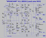
My "spooky" is very similar - plus cascodes and servo .... no .02 -.06% , but 15-25PPM @ 20Khz.
Stability wise , just the Cob of the VAS devices fall short of oscillation with this type design. I've forgot the millers - still no oscillation.
Not subjective , but I am using this now .... bass is stellar / as a stereo pair ... just "transparent". As a 20PPM amp should be.
What I "hear" is most likely the good damping factor of the EF3....
PS - a "shunted" VAS CAN affect the sound as it does increase H2/H4 at higher frequencies. Forum project "Symasym" is
liked and VAS has 100pF to earth. Much more added H2.
OS
Attachments
How a crude methode?Now C9/10 shunt through R22 (680p). Still , a crude method.
Calculate the actual load capacitance for the differential stage in your file (circuit) in the attachment, namely capacitors C13 C14, their capacitance is multiplied by the gain of cascodes Q13Q14 and Q15Q16. It’s easy to calculate the capacity.)))
As for C9/10 (680p) R22(100) - this is a frequency (1.2 MHz) that is an octave higher than the frequency of the compensation circuit at the input of the R3R4C4 amplifier, and therefore does not have a “rough” effect on the amplifier parameters.
The servo is very well made.👍and servo ....
good scheme, I think its parameters can be configured even better.My "spooky"
The parameters of the circuit are not unlimited, limiting the frequency at the amplifier input reduces the likelihood of IM distortion from the appearance of positive feedback precisely because of the limitation of the frequency properties of the transistors of the second amplification stage.is
liked and VAS has 100pF to earth.
In a single-stage version of the voltage amplifier, this will work out better than in a two-stage one.
So, let's continue the modification, or rather, return to the topology of the original version of the theme.
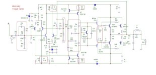
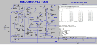
Attached is an electrical circuit, a modification “Tweak step2" from the circuit on the piece of paper, change of inclusion in the circuit of the Q5Q6 significantly improves the parameters, namely: the Q1Q2 input stage adds amplification at high frequencies with a center frequency of 44 kHz,
and the Q7Q8Q5Q6 cascade amplifies the entire audio frequency range with a cutoff frequency of 44 kHz. This gain is added up on transistors Q3 Q4 and then goes to control the output stage.
To compensate, a 2nd order filter is used, this is the electrical circuit (C11+C12)R24 and C9R21 (with additive R22R23C8).
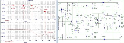
Based on the filter coefficients, this is a “type 2” Chebyshev filter.
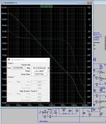
The attached diagram of the frequency response of the open loop shows the point of its influence.
the most important thing is that in such a connection, compensation does not affect the operation of the input stage, the additional gain obtained is spent largely on increasing the linearity of the operation of this input stage, and now its operation “looks” cool.
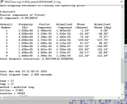
The distortion at the amplifier output at a frequency of 1 kHz is 0.004%, and at a frequency of 20 kHz - 0.012%. But it is much more important that the input stage began to work with 8 times less distortion than in the “Tweak step1 version”
Attached is an electrical circuit, a modification “Tweak step2" from the circuit on the piece of paper, change of inclusion in the circuit of the Q5Q6 significantly improves the parameters, namely: the Q1Q2 input stage adds amplification at high frequencies with a center frequency of 44 kHz,
and the Q7Q8Q5Q6 cascade amplifies the entire audio frequency range with a cutoff frequency of 44 kHz. This gain is added up on transistors Q3 Q4 and then goes to control the output stage.
To compensate, a 2nd order filter is used, this is the electrical circuit (C11+C12)R24 and C9R21 (with additive R22R23C8).
Based on the filter coefficients, this is a “type 2” Chebyshev filter.
The attached diagram of the frequency response of the open loop shows the point of its influence.
the most important thing is that in such a connection, compensation does not affect the operation of the input stage, the additional gain obtained is spent largely on increasing the linearity of the operation of this input stage, and now its operation “looks” cool.
The distortion at the amplifier output at a frequency of 1 kHz is 0.004%, and at a frequency of 20 kHz - 0.012%. But it is much more important that the input stage began to work with 8 times less distortion than in the “Tweak step1 version”
Attachments

Last edited:
It's good for my 500W sub ! It has a "brother" - the hellraiser ... (below). This is the design that forced me to use the current source servo scheme.good scheme, I think its parameters can be configured even better.
Diamond buffer (Q4/5) symmetrical designs are hard to balance offset , CFA is also hard to servo because of low impedance FB.
Just 2 22-47pF (C13/14). I omitted them when i tested , circuit just "rings" on a square - does not oscillate. 22p = 5mhz UG - 47pF = 2.5mhz
39-47p gives lots of margin , 22pF "rings a little" but at 325V/uS , CFA is fast !!
I have to use those cascodes , amp is running >65V rails. But , I can use low voltage toshiba SMD P/N matched for the diamond. whole amp runs
at +/- 11V right till cascode Q7/Q10.
This one will do <1ppm right to clip @ 1Khz.
I'm listening to STYX on these now - VERY transparent. I get to hear my ASUS XONAR DX DAC - in all it's glory...
OS
Attachments
Hennady Kovalsky - I see the emitter resistors added to the first differential. Have you checked the sensitivity to device variations in the second differential? I see very high gain for decent tracking between the complementary halves.
ostripper - You have avoided the tracking problem that complementary designs are susceptible to. 🙂
Ed
ostripper - You have avoided the tracking problem that complementary designs are susceptible to. 🙂
Ed
in fact, I don’t like it either, not because the Chevyshev type 2 approximation is used, which is still more or less phase-linear, but because for only 76dB of gain the order of compensation has to be increased.the PM does not look good between 100K and 1M, where there is still lots of gain
- Home
- Amplifiers
- Solid State
- Modification of a simple amplifier with symmetrical topology