ostripper said:...Maybe I just have a LED fetish..
...


ostripper said:...As far as heatsinks, I use what is available.
For most amps I order socket A PC heatsinks (4US$ each), line em' up screw them together , get super .1C/W good looking thermal solutions for next to nothing...
 🙂 thanks for the tip. I will try to get that to start experimenting in case reception of my ordered chassis comes late...
fab, have you looked at the following re. workability ...
1. the bias stability depends on the input FET source vagaries
2. the thermistors look like they could over-compensate
3. there's no DC offset adjustment
1. the bias stability depends on the input FET source vagaries
2. the thermistors look like they could over-compensate
3. there's no DC offset adjustment
KLe said:fab, have you looked at the following re. workability ...
1. the bias stability depends on the input FET source vagaries
2. the thermistors look like they could over-compensate
3. there's no DC offset adjustment
KLe,
1. what about the output mosfet drive transistors Q5 and Q6 mounted on output mosfet heatsink?
2. The thermistors are optional and their effect may be adjusted ( with R89/R90 values in series...
3. DC adjustment is via pots P1 and P2
What do you recommend?
thanks
fab, sorry I missed P1 and P2.
Yes, the thermistors are ok, just fiddly to get it right.
I think that the bipolar drivers will only provide 2mV/deg C T comp, but the MOSFETs require 6 mV/ deg C, that is to be perfectly coupled. I could be wrong (highly likely), but have a closer look and let us know ...
Why do you need all the LEDs?
KLe said:...
I think that the bipolar drivers will only provide 2mV/deg C T comp, but the MOSFETs require 6 mV/ deg C, that is to be perfectly coupled. I could be wrong (highly likely), but have a closer look and let us know ...
thus it looks like the thermistors could provide the missing compensation... 😉
For sure I will let you know 🙂
KLe said:...
Why do you need all the LEDs?
I like
 as ostripper suggests...😀
 But seriously, I want the jfet to have a reasonable VDS (Leds in series) and the bipolar driver will have about 20-25 ma of current (thus Leds in parallel since I am not sure if LEDs will survive for long with such a current...)

KLe said:...
I think that the bipolar drivers will only provide 2mV/deg C T comp, but the MOSFETs require 6 mV/ deg C, that is to be perfectly coupled. I could be wrong (highly likely), but have a closer look and let us know ...
I intended to screw Q5 (and Q6) on the same screw as one of the output mosfet to react more quickly to temp changes in output mosfet. I wonder if the additional thermistors will react quickly enough since the limitation of contact surface... 🙁
Can someone suggest a better tracking method?
maybe change Q5 and Q6 to v-mosfet like IRF530 (9530) or else?


Temp compensation
Thanks darkfenriz.
However, I am worried in the generally higher voltage drop (VGS ) of mosfet compared to bjt (Vbe) leading to a high reduction in jfet input stage gain because of resulting lower jfet load resistance value...
What mosfet device have you in mind?
So in this way Q5 and Q6 would not be thermally coupled to output device?
darkfenriz said:Maybe this way...
Thanks darkfenriz.
However, I am worried in the generally higher voltage drop (VGS ) of mosfet compared to bjt (Vbe) leading to a high reduction in jfet input stage gain because of resulting lower jfet load resistance value...
What mosfet device have you in mind?
So in this way Q5 and Q6 would not be thermally coupled to output device?
Temp compensation - more
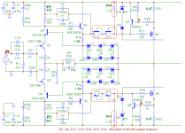
I have been playing a bit with darkfenriz idea but using a Vbe multiplier (coupled to output mosfet) instead of a mosfet. See attached circuit with Q13 and Q14 Vbe multiplier. Since voltage drop is the product of the multiplier factor and the Vbe, the Vbe variation with temp should then be also multiplied (so the sum of Q5 drop and the multiplier could be somewhere around 6mv/C (IRFP240)).
The drawback is the loss of open loop gain which I would like to avoid since it is not that high and is depending on output load impedance ...😀
Attachments

temp comp - more 1
....So I looked for a NTC thermistor (original idea) with good thermal contact with output mosfet and I have found this one attached . How can I determine the delta V / delta T ?
Is it 2% or 1% or else of rated value at 25C per deg C variation?
....So I looked for a NTC thermistor (original idea) with good thermal contact with output mosfet and I have found this one attached . How can I determine the delta V / delta T ?
Is it 2% or 1% or else of rated value at 25C per deg C variation?
Attachments
Re: Temp compensation - more
IMO you should still have a resistor in series with Vbe multiplier. 100R is enough.
fab said:I have been playing a bit with darkfenriz idea but using a Vbe multiplier (coupled to output mosfet) instead of a mosfet. See attached circuit with Q13 and Q14 Vbe multiplier. Since voltage drop is the product of the multiplier factor and the Vbe, the Vbe variation with temp should then be also multiplied (so the sum of Q5 drop and the multiplier could be somewhere around 6mv/C (IRFP240)).
The drawback is the loss of open loop gain which I would like to avoid since it is not that high and is depending on output load impedance ...😀
IMO you should still have a resistor in series with Vbe multiplier. 100R is enough.
Re: Re: Temp compensation - more
I thought I had P1 and P2 for that purpose...unless you mean in the emitter of the Vbe multiplier to reduce the variation of the VBE multiplier with temp?
darkfenriz said:
IMO you should still have a resistor in series with Vbe multiplier. 100R is enough.
I thought I had P1 and P2 for that purpose...unless you mean in the emitter of the Vbe multiplier to reduce the variation of the VBE multiplier with temp?
temp compensation
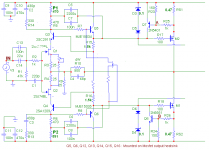
Here is another idea for themal compensation of the output mosfets. I removed the NTCs and added transistors in diode mode with bias resistor. See attached.
Vbe change of Q5 + Q13 + Q14 should equal M2 ( M4, M5) VGS change in temperature?😕
What do you think?
Thanks
Here is another idea for themal compensation of the output mosfets. I removed the NTCs and added transistors in diode mode with bias resistor. See attached.
Vbe change of Q5 + Q13 + Q14 should equal M2 ( M4, M5) VGS change in temperature?😕
What do you think?
Thanks
Attachments
Why don't you just put diodes in series with the bases of Q7, Q8, and servo the bias?
(you can always add another transistor as a limiter if you like)
(you can always add another transistor as a limiter if you like)
djk said:Why don't you just put diodes in series with the bases of Q7, Q8, and servo the bias?
(you can always add another transistor as a limiter if you like)
Hi djk
But Q7 and Q8 are the current limiter...
I am not sure I understand your suggestion unless you mean putting diodes string in parallel with mosfet source resistor?
But even that requires a lot of mosfet degeneration at source and this design does not have a lot of gain to start with (no VAS) ...Can you light up my
?Hi
Just a thought, what happens if Q1/Q2 become hotter? The negative temperature coefficient should decrease the conductance and thus the Vgs of the outputs if Q1/Q2 were sensing the output temperature, no? Not sure if it would be enough compensation, it would take careful biasing with respect to the particular J-fets and you could put the bias adjustment on the sources, but the logic seems right...... .......or maybe I just had too many beers, eh?😀
Anyway, interesting CKT.🙂
Good luck

Just a thought, what happens if Q1/Q2 become hotter? The negative temperature coefficient should decrease the conductance and thus the Vgs of the outputs if Q1/Q2 were sensing the output temperature, no? Not sure if it would be enough compensation, it would take careful biasing with respect to the particular J-fets and you could put the bias adjustment on the sources, but the logic seems right......
.......or maybe I just had too many beers, eh?😀 Anyway, interesting CKT.🙂
Good luck
CBS240 said:Hi
Just a thought, what happens if Q1/Q2 become hotter? The negative temperature coefficient should decrease the conductance and thus the Vgs of the outputs if Q1/Q2 were sensing the output temperature, no? Not sure if it would be enough compensation, it would take careful biasing with respect to the particular J-fets and you could put the bias adjustment on the sources, but the logic seems right......
Anyway, interesting CKT.🙂
Good luck
Interesting suggestion for temp compensation. Without being able to quantify the effect of thermal contact of the jfet with output trannies, if the resulting drift is different from the V-mosfet one, then I suppose that it can be difficult to adjust it and keep parts value that work at the same time....
Thanks for your interest in it !
Hi
The graphs in the datasheets for 2sk170 & 2sj74 are all at 25 degrees. I guess you would have to build a rig to measure temperature change vs conductance at a drain current suitable for the circuit, then re-calculate the resistor values. I doubt the change in conductance vs temperature is the same for any drain current. Temp co effect is usually more prenounced at larger Ids (smaller Vgs).
There has to be a better way than a Christmas tree. Would it be possible to bias a DC current through R7, R8 for the seperate single j-fet to exibit 6mV/degree change across each resistor? Re-bias the input stage acordingly? You would have to pick a suitable jfet, measure and crunch the numbers... I'm sill not completely convinced it won't work......
The graphs in the datasheets for 2sk170 & 2sj74 are all at 25 degrees.
I guess you would have to build a rig to measure temperature change vs conductance at a drain current suitable for the circuit, then re-calculate the resistor values. I doubt the change in conductance vs temperature is the same for any drain current. Temp co effect is usually more prenounced at larger Ids (smaller Vgs).There has to be a better way than a Christmas tree.
Would it be possible to bias a DC current through R7, R8 for the seperate single j-fet to exibit 6mV/degree change across each resistor? Re-bias the input stage acordingly? You would have to pick a suitable jfet, measure and crunch the numbers... I'm sill not completely convinced it won't work......Attachments
CBS240 said:Hi
The graphs in the datasheets for 2sk170 & 2sj74 are all at 25 degrees.
There has to be a better way than a Christmas tree.
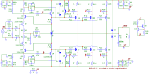
Ok, since we do not have data on the jfet temp drift, I used a bjt current source instead trying to implement your idea. I came up with that circuit where Q10 only is mounted on the mosfet heatsink to provide 2mV/C drift which must translate in 13uA that provides a delta V across R7 of 6mv (V-mosfet T drift). But doing that I had to reduce too much the jfet load so the overall gain is finally reduced...

Unless you have a different solution...
So far, the best option is the VBE multiplier in the load (with mosfet source resistor of 0.1 ohms instead of 0.47) of the jfet since the open loop gain is about 69 db giving a feedback factor of 43db. 😎 but in 8 ohms... 🙄
I like
🙂 so I put the zener there only to simplify the circuit...Attachments
- Status
- Not open for further replies.
- Home
- Amplifiers
- Solid State
- Mix of GB and F5 Amps idea