Hello,
Let me ask a few questions:
Have you finished a source with the PCB I got too?
I found some errors
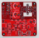
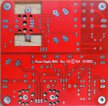
The circuit from the SB350 diodes to the 15000uF capacitors ... the plus is ok, but the minus doesn't connect anywhere. I had to modify the pcb and now of course it doesn't look professional.
Can you also provide me the wiring diagram according to the designed PCB?
Thank you
Let me ask a few questions:
Have you finished a source with the PCB I got too?
I found some errors
The circuit from the SB350 diodes to the 15000uF capacitors ... the plus is ok, but the minus doesn't connect anywhere. I had to modify the pcb and now of course it doesn't look professional.
Can you also provide me the wiring diagram according to the designed PCB?
Thank you
Attachments
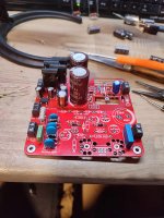
Also the negative lead of the output connector and the led are not connected to GND...and nowhere else....I have the same board as Pompiliu, it seems the pcb has to be fiddled a lot to work...It should have been nice to test one before selling, I allways do so prior to giving away. I will try tonight to figure out the mistakes. And make better photos...
....
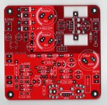
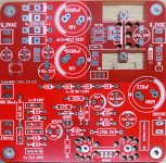
I have also a question about the preamp: why not mounting two 6.8nF series than the 3.3 nF plus 82 pf? Let's say a 3.4 nF capacitor? I don't see other reason for the 82 pf, other than augmenting the 3.3nF capacity a little bit.
....
I have also a question about the preamp: why not mounting two 6.8nF series than the 3.3 nF plus 82 pf? Let's say a 3.4 nF capacitor? I don't see other reason for the 82 pf, other than augmenting the 3.3nF capacity a little bit.
The original circuit is a classic passive RIAA stage and 3.3 and 8.2 are standard (E12) capacitor values.have also a question about the preamp: why not mounting two 6.8nF series than the 3.3 nF plus 82 pf? Let's say a 3.4 nF capacitor? I don't see other reason for the 82 pf, other than augmenting the 3.3nF capacity a little bit.
sorry, the capacitors negative connection to the ground surface on the back side actually seems to be missing!
But the solution could have been much more elegant: scrape off a bit of solder mask and
make a solder connection there, it would hardly be noticeable!

"the negative lead of the output connector and the led are not connected to GND.."
My layout program shows the connection as existing, but in the newer version from the pcb
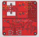
the large cutouts in the heat sink are replaced by a few holes!

But the solution could have been much more elegant: scrape off a bit of solder mask and
make a solder connection there, it would hardly be noticeable!
"the negative lead of the output connector and the led are not connected to GND.."
My layout program shows the connection as existing, but in the newer version from the pcb
the large cutouts in the heat sink are replaced by a few holes!
Last edited:
I know these, the question was if there's some other reason for the 82pF, other than a little augmentation of the total capacity - C4 and C5 are parallel conected. I don't think it could be a reason like, for example, in power supply filters where we double the thousand-ish uF capacitors with 100nF ones.The original circuit is a classic passive RIAA stage and 3.3 and 8.2 are standard (E12) capacitor values.
***
@snapper:
Yes, your drawing seems ok, but here is what we got here:
1, 2, 10, 6, 7, 8, 9, missing GND fins or simply no connection.
8.9 have connection on front, but they are not "second option" for the diodes.
That's why I connected those double diodes like I did - I used only one of the 2 diodes. Overkill, but I had them in stock, salvaged from OLD ATX PC power supplies.
3 and 4 show wrong fins, attached to the "+" eylets, instead of the "-" ones which had to go to GND.
I made the edits on scanned pictures, but the pads look strange, they are ok, silvery, as one could see in the other 2 photos.
Any (further) questions?
I have no claims, just cease insisting we didn't understand the circuit...by the way, I wish I had the exact schematic used to generate the Gerber files. I presume the mistakes are in the factory, not in your design. Unfortunately, s**t happens...
Attachments

Last edited:
I turned the 15000µf 180° compared to the original PCB, the positive terminal and diode 1+3 go to the copper surface at the top, the negative connection and diode 2+4 go to the copper surface at the bottom (ground). The board is not designed for 3-pin double diodes!
Why the ground pads are not connected is still a mystery to me, but it can certainly be easily fixed as in my previous post!
My layout program doesn't use a circuit diagram like e.g. eagle, in principle it is a drawing program with which you can copy existing layouts (sprint layout) 😉


Why the ground pads are not connected is still a mystery to me, but it can certainly be easily fixed as in my previous post!
My layout program doesn't use a circuit diagram like e.g. eagle, in principle it is a drawing program with which you can copy existing layouts (sprint layout) 😉
Sorry to dig out this old thread again, but I'd be interested in the original, tube only schematics. Is it available here at DIYAudio or anywhere else?
Best regards!
Best regards!
It can be preveiwed on Google books, see page 358:
https://www.google.co.uk/books/edit...=merlin blencowe&pg=PA358&printsec=frontcover
https://www.google.co.uk/books/edit...=merlin blencowe&pg=PA358&printsec=frontcover

 .
.- Home
- Amplifiers
- Tubes / Valves
- Merlin RIAA Preamp