Wavebourn said:
No. They were rare samples.
Sorry mlloyd got the last couple I had, I am searching for more tubes of unused ones. We can't sell them so I can give them away.
andy_c said:after my sleep gives me a new virtual posting "dick splint" 😀
Say what? 😱
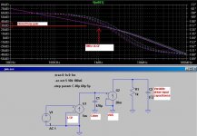
BTW, attached below is a simulation to better articulate what I’m going on about. It is simplified open loop simulation of a typical amplifier designed to a low NFB philosophy (which may also eschew Miller compensation, which is just a nice trick to maximise NFB, after all).
G1 is the input long-tail pair with a gm of 5mA/V. G2 is the voltage amplification stage, with a gm of 20mA/V. The VAS is heavily loaded with a 1k resistor and dominant pole compensation is provided by C1, shunting the output of the LTP.
The amplifier is frequency compensated for a closed loop gain of 30dB, returning a unity loop gain frequency of 1MHz. Note that for simplicity I have omitted the resistive load on the LTP, so the open loop bandwidth is not limited to 20kHz or beyond. It’s probably worth noting here that resistive loading of the VAS is not the only requirement for wide open loop bandwidth, but resistive loading of the LTP is as well – current mirrors are definitely out!
Anyway, due to the lack of feedback-compensation, such as a Miller cap around the VAS to dramatically reduce its output impedance at HF, the VAS output impedance defined by the load resistance of 1k.
C2 represents the driver input capacitance that varies non-linearly with signal amplitude. I have stepped C2 through 40pF to 60pF to show the resultant phase modulation.
Of course, you can rewire the VAS for Miller compensation (evil NFB
 ) and this phase modulation practically disappears due to the pole-splitting effect.
Attachments
G.Kleinschmidt said:I don’t buy the “swamping the non-linear load” argument. By bunging a resistor onto the VAS you aren’t getting rid of the non-linear load at all (the driver or pre-driver stage is still connected), you are just bunging a linear load in parallel with it.
The non-linear part of the VAS load is still going to cause distortion, and you’ve just added more due to the drive requirement for that added resistor.
What I was saying was only speculation, so I'm not claiming this is fact. But let me try to explain further what I was talking about with the linearization of the load by the parallel resistor. Of course the lower impedance will result in larger current drive requirements, which will increase one component of the distortion. It will also reduce the feedback, also with a detrimental effect. No disagreement there.
Anyway, consider a nonlinear resistance for which the nonlinearity is memoryless. We could take two views of this - a conductance view and a resistance view.
For the resistance view:
v = f1(i) = r * i + a2 * i2 + a3 * i3 + ...
For the conductance view:
i = f2(v) = g * v + b2 * v2 + b3 * v3 + ...
Here, f1() and f2() are inverses of each other. Do you agree that if we linearize f1() that we also linearize its inverse f2() (and vice versa)? Seeing what happens when adding a parallel resistor R1 is easier with the conductance view. When we do that, we get this result:
i = f3(v) = (g + 1 / R1) * v + b2 * v2 + b3 * v3 + ...
Here, only the linear term of f3(v) has changed relative to f2(v), and it is now larger by comparison with the nonlinear terms than it is with f2(v). If we want to translate this back into resistance form, there is of course the question of how to calculate the "a" terms from the "b" terms. It's a problem of finding the Taylor series coefficients of the inverse of a function from the Taylor series of the function. The Wambacq and Sansen book has this formula, and I could dig it out if you're interested.
Anyway, I'm not saying "I know the answer to this problem" - only trying to clarify the reasoning behind the speculation. It would be interesting to find the real answer for what has happened to several people. But also, I think that any topology for which this distortion reduction quirk occurs is probably sub-optimal.
G.Kleinschmidt said:BTW, attached below is a simulation to better articulate what I’m going on about.
Okay, I see what you're saying now.
G.Kleinschmidt said:
You have no idea what you are talking about.
One more mind reader? 😉
More linear, wider bandwidth amp needs no such feedback that requires such compensation. It's what I mean.
Glen,
you might like this one, too, a pim-sim (sic) of the F5:
http://www.diyaudio.com/forums/showthread.php?postid=1538498#post1538498
(follow the link given there, as well).
I think this is exactly your point, because the F5 VAS'es work into a lowish R paralelled with the series RC comprised of gate stopper + non-linear MOSFET C.
- Klaus
andy_c said:
What I was saying was only speculation, so I'm not claiming this is fact. But let me try to explain further what I was talking about with the linearization of the load by the parallel resistor. Of course the lower impedance will result in larger current drive requirements, which will increase one component of the distortion. It will also reduce the feedback, also with a detrimental effect. No disagreement there.
[snipped some great math for bandwidth conservation]
Andy,
Being somewhat math challenged, I reasoned as follows:
Assume that the Vas is distortionless, driving a nominally 1Megohm input Z that varies 10% thought the cycle. That causes a '10% distortion' of sorts.
Now parallel that 1 Megohm +/-10% with say 10k resistor. The total impedance variation is now 10k//1M +/-10% is around 0.1 % (admittedly cutting some corners). Thus the distortion after this trick is down from 10% to 0.1% (of sorts).
Right?
(And yes the lower impedance *may* increase the Vas distortion and thus it becomes a tradeoff as you noted).
Jan Didden
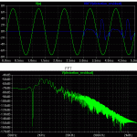
My fundamental null tool for LtSpice calculates the exact output phase before the subtraction using behavioral sources to link up Fourier integral equations
Shouldn’t be too hard from there to do something equivalent to Bob’s PIM measurement
http://www.diyaudio.com/forums/showthread.php?postid=1333137#post1333137
re calculations:
I’d have to dig it out but didn’t Cherry show the “series inversion” math in his jaes paper:
Estimates of Nonlinear Distortion in Feedback Amplifiers
Volume 48 Number 4 pp. 299-313; April 2000
jcx said:My fundamental null tool for LtSpice calculates the exact output phase before the subtraction using behavioral sources to link up Fourier integral equations
That's a great tool BTW. When I first tried it, I thought something was wrong because the residual appeared to have the same period as the fundamental. But I did a .FOUR on the residual and got a fundamental null greater than 200 dB! Great work.
KSTR said:Look here, for how to do two-tone 1:1 IMD sims:
http://www.diyaudio.com/forums/showthread.php?postid=1349571#post1349571
- Klaus
You have a simple example in the LTspice simulator? 🙂
I tried to, not work

john curl said:Sorry, PB2, it doesn't work that way. Just extra drive current.
G.Kleinschmidt said:
You have no idea what you are talking about.
I don't see how the analogy is valid here. We are talking about adding an increased load that will (especially under "swamping" conditions) dramatically increase the current swing in both the VAS and the input stage.
That WILL result in greater non-linearity from the VAS and the input stage. The only way you are likely to get a lower measured result in a real-world, closed loop amplifier with a resistive VAS load is if there is a "fortutious null" with some other non-linearity, at a specific ampitude and frequency.
Regarding the 1k Vs 1k//100k load example, with the the latter in a closed loop system you cannot neglect:
A) The increased distortion caused by a 100 fold increase in required drive current.
B) The fact that the non-linear load is still present.
Slow down Glen. I gave you a gross example, 1K//100K not to suggest that those values might represent or be used in a real amp. Just a stand alone example to point out the difference in linearity.
This seems to be pointless.
jcx said:My fundamental null tool for LtSpice calculates the exact output phase before the subtraction using behavioral sources to link up Fourier integral equations
Shouldn’t be too hard from there to do something equivalent to Bob’s PIM measurement
http://www.diyaudio.com/forums/showthread.php?postid=1333137#post1333137
re calculations:
I’d have to dig it out but didn’t Cherry show the “series inversion” math in his jaes paper:
Estimates of Nonlinear Distortion in Feedback Amplifiers
Volume 48 Number 4 pp. 299-313; April 2000
That would be a graphical representation of the distortion along with the signal output?
andy_c said:
But I did a .FOUR on the residual and got a fundamental null greater than 200 dB! Great work.
Attached:
Attachments
G.Kleinschmidt said:
Say what? 😱
BTW, attached below is a simulation to better articulate what I’m going on about. It is simplified open loop simulation of a typical amplifier designed to a low NFB philosophy (which may also eschew Miller compensation, which is just a nice trick to maximise NFB, after all).
G1 is the input long-tail pair with a gm of 5mA/V. G2 is the voltage amplification stage, with a gm of 20mA/V. The VAS is heavily loaded with a 1k resistor and dominant pole compensation is provided by C1, shunting the output of the LTP.
The amplifier is frequency compensated for a closed loop gain of 30dB, returning a unity loop gain frequency of 1MHz. Note that for simplicity I have omitted the resistive load on the LTP, so the open loop bandwidth is not limited to 20kHz or beyond. It’s probably worth noting here that resistive loading of the VAS is not the only requirement for wide open loop bandwidth, but resistive loading of the LTP is as well – current mirrors are definitely out!
Anyway, due to the lack of feedback-compensation, such as a Miller cap around the VAS to dramatically reduce its output impedance at HF, the VAS output impedance defined by the load resistance of 1k.
C2 represents the driver input capacitance that varies non-linearly with signal amplitude. I have stepped C2 through 40pF to 60pF to show the resultant phase modulation.
Of course, you can rewire the VAS for Miller compensation (evil NFB
Certainly, you can offer a highly simplified case that does not represent a real amp where the theory does not apply - and from my perspective you have.
It seems to me that the resistive component of the VAS load will be non-linear due to beta dependency on Ic, crossover effects and probably others. I was not talking about a resistor swamping capacitive effects but rather other non-linear resistive effects. Indeed, JC's example was going from 100M ohm to 1M ohm.
I'm not suggesting that anyone would do this but to make your sim more representative of the effect put 6000pF (linear) in parallel with the 1K on the VAS. Then show your sim results with the *same* stepped capacitance.
Also, you show the effective Cdom as a linear cap to ground as I interpret your diagram. A non-linear Miller cap (device capacitance) that actually sees the gain of the VAS is also more representative of the real circuit and the effects that we are looking for.
PB2 said:
Also, you show the effective Cdom as a linear cap to ground as I interpret your diagram. A non-linear Miller cap (device capacitance) that actually sees the gain of the VAS is also more representative of the real circuit and the effects that we are looking for.
Right. And Bob Cordell still did not answer why feedback should create PIM in case of constant C, but reduce it in case of non-linear C.
janneman said:
Andy,
Being somewhat math challenged, I reasoned as follows:
Assume that the Vas is distortionless, driving a nominally 1Megohm input Z that varies 10% thought the cycle. That causes a '10% distortion' of sorts.
Now parallel that 1 Megohm +/-10% with say 10k resistor. The total impedance variation is now 10k//1M +/-10% is around 0.1 % (admittedly cutting some corners). Thus the distortion after this trick is down from 10% to 0.1% (of sorts).
Right?
(And yes the lower impedance *may* increase the Vas distortion and thus it becomes a tradeoff as you noted).
....and –40dB loop gain + the extra current swing required of the LTP.
That is exactly what PB2 said with the speaker analogy. It is intuitively easy to imagine the resulting voltage developed across the added resistor of an open loop amplifier being more linear, but I think this leads to a wrong conclusion about what happens when the loop is closed.
I wish I could explain this better, but what I have found when trying to get the lowest THD from a simulated topology in SPICE is that what defines the resultant output spectrum is the magnitude of the non-linearity of the error signal. Whenever you increase the loading on the VAS, you just increase the magnitude of that non-linearity (imagine the residual THD signal in both cases of your example with the fundamental removed).
Also, a 10k resistive load will make VAS linearity in just about any moderately refined design mediocre at best.
KSTR said:Glen,
you might like this one, too, a pim-sim (sic) of the F5:
http://www.diyaudio.com/forums/showthread.php?postid=1538498#post1538498
(follow the link given there, as well).
I think this is exactly your point, because the F5 VAS'es work into a lowish R paralelled with the series RC comprised of gate stopper + non-linear MOSFET C.
Thanks Klaus.
I think that if a designer is paranoid about PIM, the VAS collector-to-output stage interface is the first place to do things right. After all, going along the chain in a typical design, that is the first place where a real substantial, non-linear capacitive load is encountered.
To me, some sort of feedback compensation is mandatory here, to get the VAS output impedance at HF as low as possible.
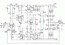
 Now would everyone agree that Otala's VAS and chosen frequency compensation scheme (working into only a double EF) is somewhat sub-optimal, from a PIM perspective?
 Attachments
PB2 said:
Certainly, you can offer a highly simplified case that does not represent a real amp where the theory does not apply - and from my perspective you have.
It seems to me that the resistive component of the VAS load will be non-linear due to beta dependency on Ic, crossover effects and probably others. I was not talking about a resistor swamping capacitive effects but rather other non-linear resistive effects. Indeed, JC's example was going from 100M ohm to 1M ohm.
I'm not suggesting that anyone would do this but to make your sim more representative of the effect put 6000pF (linear) in parallel with the 1K on the VAS. Then show your sim results with the *same* stepped capacitance.
Also, you show the effective Cdom as a linear cap to ground as I interpret your diagram. A non-linear Miller cap (device capacitance) that actually sees the gain of the VAS is also more representative of the real circuit and the effects that we are looking for.
Wow, you completely miss the point. Your 6000pF suggestion makes no sense. What driver transistors have that much input capacitance? And as explained, C1 (Cdom) is a SHUNT compensation cap.
The fact that I stepped the load capacitance linearly doesn't matter at all - it was just to show the magnitude of phase modulation at will occur with a small variation in VAS load capacitance if the VAS output impedance at HF is in the order of 1k (as in the Otala amp, just for example).
This is the PIM issue I was replying to Andy about, and it has nothing to do with the new discussion about a VAS load resistor swamping non-linear load effects.
Also, if you think that my simplified simulation is not representitive of a real life, workabe amplifier, I can draw the amplifiers full schematic diagram for you.
G.Kleinschmidt said:
He used his way to skin the cat. Very creative, by the way, instead of copying and pasting from textbooks and online forums.
I personally would hesitate to use 3 stages surrounding them by feedback, though it was common then in tube amps that did not need so deep feeedback to sound properly.
Wavebourn said:
He used his way to skin the cat. Very creative, by the way, instead of copying and pasting from textbooks and online forums.
I'm sorry, this is a technical discussion. Do you have a technical answer?
G.Kleinschmidt said:
Well, it's certainly sub-optimal from a distortion perspective. But for me at least, it's not easy to see how much of the distortion of the closed-loop amp is PIM and how much is AIM. OTOH, I think the distinction is vastly overrated. Basically, I think PIM is interesting as a thought experiment and not much more.
- Home
- Amplifiers
- Solid State
- Matti Otala - An Amplifier Milestone. Dead or Alive