> thinking about the heat dissipation
The signals at the jack are part-Volt. WTH do you need a 280V supply?
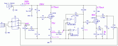
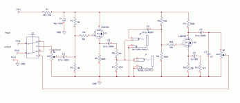
From clean sheet I would pad-down first (since this may be coming from a clipping tube stage). However I don't feel like re-drawing. Still the pad may usefully be made part of the driver. And even if you only have 300V power, you can drop a lot on-board so the transistors don't cook. I also would not use R13 (or not so small) if you have to pad-down after. C5 may be smaller than best bass response needs.
The signals at the jack are part-Volt. WTH do you need a 280V supply?
From clean sheet I would pad-down first (since this may be coming from a clipping tube stage). However I don't feel like re-drawing. Still the pad may usefully be made part of the driver. And even if you only have 300V power, you can drop a lot on-board so the transistors don't cook. I also would not use R13 (or not so small) if you have to pad-down after. C5 may be smaller than best bass response needs.
Attachments
I've fiddled with KiCad a little myself, enough to generate simple schematics, but no PCBs yet. I continue to struggle with KiCad, with the software winning the battle much of the time!...I tried KiCad instead...
Increasing C5 will bump up the deep bass response a bit. You might try 2.2 uF there instead of 1 uF. That will get you to 50 Hz at (-3 dB), so should be plenty for guitar which doesn't go below 82 Hz.I didn't dig deeper for any time constants or similar things.
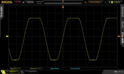
True, though you have a massive 260 volts peak-to-peak output by then, so it may not matter in a practical sense!What I will definitely try to do is to make the the return stage more symmetrical. You can see from the picture that the reference 0V line doesn't sit in the middle of the waveform.
But if this bothers you, you can decrease the "Return" LND 150 source resistor a little. In your last circuit diagram, that's R12 (22k). Try 15k there instead - that should get you very close to symmetrical clipping, and you should have over 290 volts p-p output at that point. 😱
-Gnobuddy
This comes down to personal preference. 300 volts DC is conveniently available, most 9V FX pedals can put out up to 6 volts peak-to-peak, and typical (half-12AX7) recovery-stage gain is 50x.)The signals at the jack are part-Volt. WTH do you need a 280V supply?
Put together, that means if the FX recovery amp can cope with 300 volts p-p output, the FX loop is very unlikely to ever clip, even fed from an overenthusiastic distortion pedal turned up to maximum gain and maximum output level.
Is this absolutely necessary? Probably not. But is it a bad thing to have the extra headroom? Probably not.
I assumed the loop output would drive either a normal 12AX7 gain stage, or a long-tailed-pair phase splitter. The first of those will typically accept nearly 4Vpp before it starts to clip, the LTP will need twice that, or 8V pp.I also would not use R13 (or not so small) if you have to pad-down after.
R13 was chosen to provide a voltage gain of 50x, bringing a nominal 100 mV RMS signal at the "Return" jack up to 5 volts RMS at the MOSFET drain. Enough to just clip the subsequent stage, if that is desired.
Cobretti is the only one who knows exactly what comes before or after the FX loop, so he's the only one who can make a more informed set of design choices.
Here's that subjective thing again - overpowering woofy bass, or a more balanced guitar tone?C5 may be smaller than best bass response needs.
I chose C5 for (-3 dB) at 82 Hz, as seen in the LTSpice simulation I posted, and I consider this more than adequate. But not every guitar player agrees, including both you and Cobretti. So both of you will want a fatter cap there.
-Gnobuddy
Thanks for your help guys. I have changed the 47K R5 to 100K. It did help to reduce some heat of the Q1 transistor, but the transistor is still hot, but nothing to worry about I guess. I have also reduced the R12 to 15k as Gnobuddy suggested and the output is now more symmetrical. I didn't resolve the low frequency roll off yet but I think it might be coming from the SEND stage around Q1. The small (78 mVrms when testing) sine wave on the SEND jack seemed some kind of refined - more sinusoidal compared to 3.4Vrms signal coming from the treble potentiometer side, that I distorted on purpose so I can compare in and out. I hope I am not dealing with something stupid like those plated contacts on the Neutrik jacks, are they fooling me? I was recently reading about ferrous materials in signal path in SS amplifiers, especially magnetic banana binding posts can ruin your day when you do your low THD measurement, the number can change by order of magnitude.
Attachments
Yes, it should be fine. Approx 1.5 mA, a bit over 150 volts from drain to source, so under 250 mW power dissipation. This should be fine - typically, the TO92 package can dissipate up to 600 mW before the semiconductor inside cooks, so you are now operating at less than half of maximum dissipation....Q1...still hot, but nothing to worry about I guess.
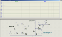
If you used the values in your last schematic, no it is not the send stage. See attached LTSpice simulation, which shows both the send and return stages are flat from below 80 Hz to beyond 10 kHz, which covers the full guitar range.I didn't resolve the low frequency roll off yet but I think it might be coming from the SEND stage around Q1.
I chose the "Return" MOSFETs 1 uF source bypass cap to cause very slight bass loss at 82 Hz. As I mentioned earlier, you can increase this to 2.2 uF if you want to eliminate the very slight bass loss (I did this in the LTSpice sim attached to this post.) Or just go for massive overkill and plug in a 10uF, 25V electrolytic capacitor, positive terminal to the MOSFET source.
Speaking of which, there is nothing wrong with electrolytic caps. Every famous piece of music you ever heard has passed through dozens of electrolytic caps before it reached your ears - they are in every classic guitar amp, every mixing desk, every microphone preamp. Just about every analog piece of audio electronics is full of aluminium electrolytic caps, except for a few overpriced toys sold to audiophiles with too much money and too little knowledge.
You can also use multi-layer ceramic caps (MLCC), which are now available up to 25uF or so, at low cost. They are excellent capacitors, compact, affordable, and work very well. Get the through-hole versions, unless you're prepared to deal with SMD components!
The source impedance is much lower on the Send jack, and I'm guessing that reduced the amount of hum and noise pickup that the oscilloscope was seeing.The small (78 mVrms when testing) sine wave on the SEND jack seemed some kind of refined - more sinusoidal compared to 3.4Vrms signal coming from the treble potentiometer side
Neutrik jacks have a long history of excellence. Plated contacts are a good thing, as that reduces corrosion, reduces contact resistance, and extends contact life.I hope I am not dealing with something stupid like those plated contacts on the Neutrik jacks
I have never had a problem with a new Neutrik. Like all jacks, they will eventually fail, usually after ten or twenty years, but that is to be expected. Mechanical parts always wear out eventually.
Please be very, very skeptical. Sad to say, most of what you read on audiophile forums is complete nonsense.I was recently reading about ferrous materials in signal path in SS amplifiers, especially magnetic banana binding posts can ruin your day when you do your low THD measurement, the number can change by order of magnitude.
-Gnobuddy
Attachments
Indeed. The small percentage who are trying to measure and then understand the physics of what they are hearing (and there's a few of them hereabouts) are drowned out by those whose level of understanding is, frankly, at the "cargo cult" level :-( But that's hi-fi marketing for you.Please be very, very skeptical. Sad to say, most of what you read on audiophile forums is complete nonsense.
Thank you Gnobuddy for the simulation. FX loop is good now, it sounds good as well and I will leave it like that. No reason to change anything. I am aware of audio foolery nonsense, and I have basic understanding of physics. However, to have a ferrous material in signal path, like for example speaker cable spades and poor quality binding posts will introduce measurable THD difference. The DUT itself has to be in low THD numbers to begin with of course. If a good sound card (Lynx for example) or Audio Precision is used for THD measurements, then, it can really be detected. We are talking about 0.0001% of a difference which has nothing to do with tube amps ofcourse. When I find the link, I will post it here. Thanks again.
Thanks for posting the link!
Unfortunately the article is behind a paywall and is definitely not worth $33 USD to me, so I can't read it. But no matter - as you said earlier, whatever effects are described in the paper are going to be far below the ability of the human ear to discern, and therefore, utterly irrelevant.
One of the things that continues to bewilder me is that people chasing some imaginary Hi-Fi holy grail will obsess over 0.0005% THD from their amplifier, while entirely ignoring the twenty thousand times larger 10% or so THD from their loudspeaker system. 😱
-Gnobuddy
Hi guys. I read everything. I try to understand how you choose the values for the CS amplifier in the return side. Let's say I have a 300V supply and an lnd150. I want the maximum AC voltage gain, I understand I have to bias the mosfet as symmetrical as possible to have the lowest distortion. But can it get get the maximum swing with any Id ?
Do you choose the gate voltage arbitrarily (20V why not 60V, or half the supply) ? Any gate voltage will give me the same gain ?
I understand the gate voltage is used to bias the mosfet with Rs source to an Id, but why did you set Id to 1.3mA (with the 15K) ? why not 2mA ?
Thank you for your knowledge.
In 1948, getting enough voltage gain was difficult. Even relatively new "high gain" triodes like the 6AV6 (identical to one of the two triodes in a 12AX7) struggled to get a voltage gain of fifty times (34 dB) in a practical circuit.Let's say I have a 300V supply and an lnd150. I want the maximum AC voltage gain
That was more than seventy years ago. Modern semiconductor devices have enormous amounts of gain available. Left to itself, an LND150 will give you too much gain - far too much to be usable. So we definitely don't want the maximum voltage gain we can get from it!
Instead, we need to lower the gain from its maximum, and set it to the value we want. In this circuit, this is done by only partially bypassing the source resistor. R13 (1.5k) keeps C5 from ever completely bypassing R12. (The numbers are from Cobretti's latest schematic, in the post immediately after yours.)
Not exactly - the distortion will already be low because of the negative feedback at the source due to R13. The point of biasing symmetrically is to increase headroom, not gain: you can put a bigger signal through the stage before it clips when it's biased symmetrically....I have to bias the mosfet as symmetrical as possible to have the lowest distortion...
Within reason, yes. You could bias it to 100uA or 2 mA, and it would still work. (But there may be other problems to deal with, see below.)But can it get get the maximum swing with any Id ?
The problem with FETs is that they have wide production tolerances. Vgs(off), the voltage at which an FET turns fully off, varies up to 300%, even 500%, between two supposedly identical FETs.Do you choose the gate voltage arbitrarily (20V why not 60V, or half the supply)?
How do you keep this variation from ruining your circuit? You bias the source to a DC voltage much larger than than the changes in Vgs_off. If Vgs_off varies by, say, up to 2 volts between one LND150 and another, then if we bias the source to 20V, those +/-2 volt changes only affect the source current by about 10% (because 2 volts is 10% of 20 volts.)
This is not terribly critical. The circuit would work fine if you picked 30V instead. But you would have slightly less output headroom, because the drain can now only swing between +30V and +300V (instead of +20V and +300V). This probably doesn't matter at all, as we have plenty of headroom in this circuit, by deliberate design.
Not exactly. With BJTs (and to a slightly lesser extent, FETs) you get more voltage gain if you have more DC voltage across the collector (or drain) resistor! An FET running on a 9V supply with 4V across the drain resistor will have less gain than the same FET running at the same current on 300 volts with 150 volts across the drain resistor.Any gate voltage will give me the same gain ?
In this circuit, the more we raise the gate voltage, the less DC voltage is available across the drain resistor (especially when we want maximum headroom, i.e., symmetrical clipping limits.) However, we have a full 300 volts DC to play with, so nothing is very critical.
2 mA would work too. The LND150 would run hotter, though.I understand the gate voltage is used to bias the mosfet with Rs source to an Id, but why did you set Id to 1.3mA (with the 15K) ? why not 2mA ?
Simple audio circuits like this one are much easier to design with semiconductors (rather than valves). No need for load lines, no struggling to get enough gain, et cetera.
-Gnobuddy
I don't know how to thank you enough. But Thank you!
I read you post almost 20 times to digest everything,
thank you for taking the time to write everything.
Let's see, I will do a step by step design for 400V and 5% variation :
-1- Check Vgs(OFF) : it's 2V variation for the lnd.
I will set the voltage divider to 40V=5%. 10M and 1M give 36.5V, pretty close.
-2- Let's say I bias the mosfet at 1.5mA, ohms law give a resistor of 24K for 36.5V.
Now my source resistor is 24K.
-3- It's time to choose the Drain resistor.
I should have 400V-36.5V=364.5V of swing peak to peak. And 1.5mA current.
The gain is set by the voltage across R drain. So the higher the R the higher the Voltage gain.
But how should I choose R drain for symmetry ?
Should I set the drain voltage to half the available voltage swing ?
Is is the wrong way/steps to design it ? Can I have a real world example ?
It's almost understood. Sorry I am still learning.
If you're going to bypass the source resistor (with a capacitor), yes; the bigger Rd is, the more (open-loop) voltage gain you get.-3- It's time to choose the Drain resistor.
I should have 400V-36.5V=364.5V of swing peak to peak. And 1.5mA current.
<snip>
The gain is set by the voltage across R drain. So the higher the R the higher the Voltage gain.
But: a very big Rd also raises output impedance (it will be roughly equal to Rd.) Depending on what sort of load this circuit will be driving (long shielded cable, for instance), too high an output impedance may not be desirable. So it's something to keep in mind.
The other thing is headroom. If you choose Rd to have 350 volts DC across it, your output can swing 350 volts positive, but only some 12-13 volts negative before clipping. If you only need, say, 1 volt RMS output, this may be fine. But if you want lots of input headroom, or a large undistorted maximum output voltage, then this wouldn't be a good bias point.
Exactly! It's just Ohm's law in action. Peak-to-peak voltage is 360 volts in your example, half that is 180 volts, and you have 1.5 mA of drain current. So R = 180/1.5^(-3), or 120,000 ohms. 120k, in our usual short-hand.But how should I choose R drain for symmetry ?
Should I set the drain voltage to half the available voltage swing ?
I would also check power dissipation in the FET, just to be sure it's safe. You have a 400V supply, 180 volts dropped across Rd, and 37 volts dropped across Rs. That leaves 183 volts across the FET, and 1.5 mA current. Power dissipated is 275 mW. This is well within the dissipation capability of a TO92 package. (The device will usually burn to death at about 500 - 600 mW according to the datasheet, I usually aim for 250 mW or less to keep the device cool and reliable.)
Nothing to be sorry about at all! 🙂It's almost understood. Sorry I am still learning.
Have you tried playing with LTSpice? It's free, and you can learn a lot by building and simulating virtual circuits. There is a very nice set of LTSpice tutorials on the 'Web by Simon Bramble to get you started.
-Gnobuddy
You don't know how grateful I am.
I looked everywhere for help, so thank you very much.
I downloaded ltspice, I already used it last year I understand this program but I completely overlooked it.
I will simulate this circuit, because today I found out that the lnd will probably not accept 3.5Vpp.
I will try to find another mosfet, but I don't know if I should change the mosfet or try another circuit ?
Do you have a preferred mosfet you use for high signal ?
But really thank you very much Gnobuddy.
If I was in canada I would have send you a present.
...can it get get the maximum swing with any Id ?....
The drain current should be much larger than the LOAD current.
Many beginners forget that the amplifier has to drive a load.
In resistance-coupled amplifiers we use a rule of thumb: plate (or drain) resistor 2X to 5X smaller than load. This ensures the load can be driven to a large fraction of the supply voltage.
In the plan a few posts above the apparent load is a 1Meg pot. However it may be driving a 200k grid resistor, or stray capacitance of similar impedance at the top of the audio band. 200k||1Meg is 167k. So by the 2X-5X rule we want Rd like 83k to 33k. However we have 300V supply and need less than 1V signal, so it isn't critical. 100k is a nice round value, used a lot as Fender plate resistors, stage DC current is reasonable.
You're very welcome! 🙂I looked everywhere for help, so thank you very much.
Between the ages of 8 and 20, I was constantly reading electronics books, and everything I've been writing about here came from one or more of them. Many of those books were written before MOS technology, so no MOSFETs, but the fundamental concepts of biasing a JFET or BJT are not that different.
Excellent, I think that will help you a lot. You will need to find and download an LTSpice model for the LND150. Or you can use the one I'm attaching to this post (save it as "LND150.txt" in the same folder as your LTSpice simulation, and remember to use ".include LND150.txt" in your simulation....ltspice...I already used it last year...
This isn't correct...I will simulate this circuit, because today I found out that the lnd (LND150) will probably not accept 3.5Vpp.
It's true that you cannot apply 3.5Vpp to an LND150 gate - if the source is fully bypassed, or connected directly to ground.
But in the circuit shown here, that is not the case. We have a 1.5k resistor (R13) providing negative feedback at the source, remember? The result of this is that most of your input signal will actually appear across the 1.5k resistor, and only a small fraction of it will appear between the gate and source of the MOSFET. So the MOSFET won't overload.
This particular circuit has a maximum output voltage a little less than 300 Vpp. It was designed to have a voltage gain of approximately x50, to roughly match a half-12AX7 triode gain stage. Put those two numbers together, and the maximum input signal should be close to 6 Vpp. More than that, and the output will clip.
If you have a different application in mind, you can always change resistance values to increase input headroom. Remember, you are NOT limited by the Vgs_off of the FET! Instead, you are limited by the power supply voltage, and the voltage gain you need from your circuit.
Thank you, I appreciate the thought!If I was in Canada I would have send you a present.
Considering all the ugly and scary world news we are hearing about these last few days, living in Canada already *is* a present! (And so is living in Italy!) 🙂
-Gnobuddy
Attachments
A year or two ago, pondering the (small) load-driving ability of an LND150, I looked to see if there was a P-channel, roughly complimentary part.Many beginners forget that the amplifier has to drive a load.
I found one - TO-92 package, up to 500 volts between source and drain, P-channel, depletion mode MOSFET. I forget the part number, though.
So if we wanted we could go one step closer to a primitive op-amp topology by adding complimentary source-followers to the output, biased a milliamp or so into class A for simplicity. If the output pair was an LND150 and its (roughly) complimentary P-channel alter ego, current is still limited to a milliamp or three, but at least the source impedance would be low. (And, of course, there are beefier MOSFETs available if desired.)
In this particular circuit, though, it seemed to make sense to just use a 100k drain resistor and be done with it, just as you might have done with a half-12AX7 instead.
-Gnobuddy
> P-channel, depletion mode MOSFET. I forget the part number, though.
Google can't find it. If you remember, post it.
However there's no compelling reason for depletion mode. Thousands of power amps have been built of enhancement mode devices. A tiny pair is MicroChip TC1550.
http://ww1.microchip.com/downloads/en/DeviceDoc/tc1550.pdf
There's no power rating. However surely 100mW dissipation. In AB mode that's good for 200mW of output. Or 100Vrms into 50k.
Of course if you are interfacing <1V FX loops then a 300V supply is grossly excessive. For more than one stage of that it would make sense to add a 15VDC supply and use more mundane jellybean parts.
Either I'm delusional, or the part has gone away. I thought I remembered a part number beginning with "Z" and followed by a long string of numbers, but I can't find it at Digikey or Mouser. Like the 200 million year old, 23 foot long, Chinese Paddlefish, it appears to now be extinct. 🙁 ( Chinese paddlefish, one of the world's largest fish, declared extinct )If you remember, post it.
Very true, and the Supertex VP0550N3-G ( https://media.digikey.com/datasheets/production/1610171/1/VP0550.html ), Microchip VP2450 ( https://media.digikey.com/datasheets/production/1610175/1/VP2450.html ), and Diodes Incorporated ZVP0545A ( https://www.diodes.com/assets/Datasheets/ZVP0545A.pdf ) all look like possible options; all three can tolerate typical tube guitar amp B+ voltages, and all are available in TO-92 through-hole packages.However there's no compelling reason for depletion mode.
That is an interesting beast!A tiny pair is MicroChip TC1550.
I don't think Cobretti ever specified what the desired output signal level was. I assumed it could be anywhere from 4 Vpp (to fully drive a half-12AX7 gain stage) to 70Vpp (to fully drive a cathodyne phase-splitter.)...if you are interfacing <1V FX loops then a 300V supply is grossly excessive. For more than one stage of that it would make sense to add a 15VDC supply...
While the nominal "instrument level" signal from a guitar pedal is 100 mV, any member of Spinal Tap could easily achieve 6 Vpp from his ThunderThrobber Maxblood distortion pedal powered by the usual 9V, simply by turning up gain and output level knobs to eleven.
At the same time, assuming 30 mV in (from a more refined guitarist) and a voltage gain of x50 gives you about 5Vpp output...just about right for a subsequent half-12AX7 gain stage. And a voltage gain of x50, combined with a maximum input of 6 Vpp, requires a B+ voltage of 300 volts.
So I don't think running the FX loop in a tube guitar amp on 300 VDC is a terrible idea, though 100 Vdc might have made some things easier. I think having a large power supply voltage here allows the FX loop to have one of the nice features of a tube guitar amp - lots of headroom before clipping, which in turn guarantees no nasty solid-state distortion from the FX loop.
-Gnobuddy
- Home
- Live Sound
- Instruments and Amps
- Marshall FX loop