So I checked all transistors and the rest of the resistors, diodes and caps on P501, and they all checked out ok
I had some 100ohm resistors so I changed R526 and had a go. Looks like its OK. No weird behavior or strange measurements. Think I'm going to order the non polarized caps, some new caps for P501 and a resistor with proper wattage.
So I have another question if I may..... In near future I really need a pre-out in my amp and wanted to build one into this one. Was thinking about taking it out from J502 on P501 board. Question is - do I need to build a buffer?
Are you saying the amp is now fully powering up with all boards connected ?
J502 on board p501 is fed from buffers so yes that should be fine for a pre out without additional buffers .
J502 on board p501 is fed from buffers so yes that should be fine for a pre out without additional buffers .
Are you saying the amp is now fully powering up with all boards connected ?
J502 on board p501 is fed from buffers so yes that should be fine for a pre out without additional buffers .
Yes, all boards connected and amp is powering up with no issues. Only thing is, I've not re-soldered the two last pairs of power transistors yet (Q731, Q733, Q732 and Q734). Have not activated class A, and bias pots are still on minimum
J502 on board p501 is fed from buffers so yes that should be fine for a pre out without additional buffers .
Nice! Thanks. Is this the buffer circuit? Of some unknown reason I was hung up in that a buffer was made up from opamp circuitry
Attachments
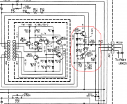
What you have circled is the output stage of one of the discreet opamp type circuits , the whole thing includes the rest of the circuit in the above photo . More correctly the whole of the above is one of the 2 preamp gain stages which offers buffering to the next stage . Strictly speaking a buffer is a unity gain stage able to drive a lower impedance than the preceding circuitry so yes the circuit circled is a buffer but it exists with the rest of the circuit , like the power transistor part of the main amp boards .
Last edited:
What you have circled is the output stage of one of the discreet opamp type circuits , the whole thing includes the rest of the circuit in the above photo . More correctly the whole of the above is one of the 2 preamp gain stages which offers buffering to the next stage . Strictly speaking a buffer is a unity gain stage able to drive a lower impedance than the preceding circuitry so yes the circuit circled is a buffer but it exists with the rest of the circuit , like the power transistor part of the main amp boards .
I think I get what you're saying, although I feel impared by my lack of knowledge. After doing some googling I see what happend. I've been reading about buffering preamp outputs to isolate and not impose impedance variations to existing circuitry. I did not however look at other than integrated opamp examples, so I could not see the buffer (symbol) per se in the preamp circuit - if this ramblin made any sense 😕😉
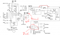
So concidering the block diagram, is this about right regarding exixting buffering?
Attachments
PS forgot to say good news on the amp 🙂
Thanks! I feel close, but will hold off the celebration to there is actual sound passing through. One thing is for sure, I could NEVER have done this without your help! It's very much apreciated. Wish I could buy you a beer 😀 Also a big thanks to others that have contributed
Ref Post 127 what you have circled are the preamp gain stage and the main amp gain stage both of there outputs offer buffering , one to drive the tone control stage and the other to drive the speakers . As I say if you reduced there gains to unity you could call them buffers .
After doing some googling I see what happend. I've been reading about buffering preamp outputs to isolate and not impose impedance variations to existing circuitry.
Yes but the output impedance of the preamp circuitry at J502 on board P501 means you should not require an additional buffer unless you want to drive a low impedance , anything 10K ohm and above should be fine .
Got it. So basically a buffer is much the same as a amp circuit, but without the gain.
Edit;
Which is what you explained in your above post. Sorry for needing to be spoon fed basic stuff, I'm a bit sleep deprived these days
Edit;
Which is what you explained in your above post. Sorry for needing to be spoon fed basic stuff, I'm a bit sleep deprived these days
Last edited:
Amp is now completed with new caps on pre amp board and non polarized caps on main amp board. I've also soldered in the last pair of power transistors.
It powers on and comes out of protection mode every time. Did some tapping with a wooden dowel. Remains to adjust bias and try class A switch, and then it should be ready for some proper testing
It powers on and comes out of protection mode every time. Did some tapping with a wooden dowel. Remains to adjust bias and try class A switch, and then it should be ready for some proper testing
Last edited:
I did some bias adjusting with bulb limiter, so I aimed lower than spec. There's a issue with negative side on L channel. Bias voltage is aprox. 8-10mV higher than positive side. DC offset is higher than spec as well, but only around 4-5mV.
I checked all voltages around the junctions (a lot of -0,6V values) and all other I could find on schematic working back from power transistors. Only thing that is a bit off is around the input(Q701), but I'm not sure this affects bias current much
I checked all voltages around the junctions (a lot of -0,6V values) and all other I could find on schematic working back from power transistors. Only thing that is a bit off is around the input(Q701), but I'm not sure this affects bias current much
Assuming you have been measuring correctly, i.e. across each 0.18 ohm resistor:
If that's with the output unloaded and no substantial output DC offset, how could you have a difference in bias there? Bias current could only be flowing from B+ through the outputs, emitter resistors and back into B-. Mr. Ohm would like to suggest that one of your resistors must have gone high. Check all 4.
And no, bias and DC offset should be pretty much independent.
If there is excessive output DC offset, it could be a lot of things - R709 (27k) does not match R703, leaky / damaged C711 (possibly C713), R713 and 715 (220R) do no match, and of course a damaged Q701 (2SC3067). After a meltdown, the capacitor in the feedback network and the feedback-side input transistor are common casualties.
Looks like you can still get 2SC3067s in this peculiar bug-shaped DIP-6 here and there if you need to replace Q701. If you have a pair of KSC1845s in stock, you could epoxy those together (same orientation) and use that for testing or a half-decent substitute even. Just for testing, just about anything with an ECB pinout and at least ~80 V of Vceo would work... 2SC2240s for sure, even BC639s. With this being a folded cascode input, transistor type should be substantially less critical than in some other amps.
I did some bias adjusting with bulb limiter, so I aimed lower than spec. There's a issue with negative side on L channel. Bias voltage is aprox. 8-10mV higher than positive side. DC offset is higher than spec as well, but only around 4-5mV.
Check across both ceramic resistor pairs on the L channel , its probably just a slight mismatch with current sharing between output transistors now that you have both pairs of outputs in circuit now .
Is that 4-5mV total offset voltage if so that's good don't expect zero offset .
its probably just a slight mismatch with current sharing between output transistors now that you have both pairs of outputs in circuit now .
Correction I forgot the setting is only 18mV total across 2x 0.18ohm , so 9mV difference suggests one of the output trannies is not conducting . check across all four 0.18ohm resistors on the left channel and recheck the continuity of the ceramic resistor combinations as " Sgrossklass " suggested .
Ps points towards the latest connected output pair/resistors on the left channel .
Last edited:
Never mind, I'm just being stupid.... I've done so many measurements with 0V/ground as reference, but obviously this is not the right way to measure bias. What I wrote in my last post don't make much sense. Bias is now correctly adjusted, AND measured 😉
Regarding DC offset I have aprox. 3-4mVneg at both channels.
Input side (Q701 and Q704) is a bit off. Emitter voltage is -0,6V (close to 0,7V spec) The two Base voltages are lower, at 80-90mVneg.
Regarding DC offset I have aprox. 3-4mVneg at both channels.
Input side (Q701 and Q704) is a bit off. Emitter voltage is -0,6V (close to 0,7V spec) The two Base voltages are lower, at 80-90mVneg.
Never mind, I'm just being stupid.... I've done so many measurements with 0V/ground as reference, but obviously this is not the right way to measure bias.
Its been a long journey 😉
The two Base voltages are lower, at 80-90mVneg.
80-90mV over 27K equates to approx. 3uA of base current absolutely fine .
- Home
- Amplifiers
- Solid State
- Marantz PM-80mkII issues (I'm sorta stuck)