I wonder whether "cheap" generic inks have any bearing on this. (Edit... not saying you are using those, just wondered) I use Jettec cartridges which are guaranteed as good as originals.
As doctordata says, check your print settings (see fourth image in post #1). You must turn the contrast up and perhaps turn brightness down although I found that made little difference tbh. Select "Best Photo" which prints the finest detail and the most slowly.
As doctordata says, check your print settings (see fourth image in post #1). You must turn the contrast up and perhaps turn brightness down although I found that made little difference tbh. Select "Best Photo" which prints the finest detail and the most slowly.
In a sort of transition period when we moved from ink and crepe tapes to PC and plotter/ printer, ca 1990 or so, I used ordinary laser foils, but getting enough contrast and fill was always a problem, so I often resorted to stacking several foils,- not good for very thin lines, though.
That problem was solved when i found he laserstar foils with it's slightly matte surface.
I've never used the Jetstar foils, but they look very similar.
FWIW,- the Lasestar foils looks and feels VERY similar to the polyester drafting films we used way back then.........
That problem was solved when i found he laserstar foils with it's slightly matte surface.
I've never used the Jetstar foils, but they look very similar.
FWIW,- the Lasestar foils looks and feels VERY similar to the polyester drafting films we used way back then.........
I also have a feeling that my UV tubes might be the incorrect wavelength. I usually need about 8-10 minutes of exposure which is a long way off the 3 minutes that Mooly suggests.
The light sorce should have it's main energy around 400-420 nm, socalled actinic or actinious light. I'm pretty sure that the Osram designation for the typical 15W 50cm tubes used in most lab UV boxes was TLA-15, but I'll have to check that. Google didn't help this time. Check Mega UK, Bungard.de etc etc Several regular parts distributors also sell '' protoyping '' equipment. I'll check when I get back to work, but most likely that won't untill end of next week, because of other tasks.
I'm presuming that these will be the correct ones ?
Buy UV Exposure Units - Replacement Tube & Starter Kits AR52, UV Exposure Unit - Starter Kit, 15W CIF AR52 online from RS for next day delivery.
They are 365nm though.
Buy UV Exposure Units - Replacement Tube & Starter Kits AR52, UV Exposure Unit - Starter Kit, 15W CIF AR52 online from RS for next day delivery.
They are 365nm though.
That looks just about right..... 🙂 and darn cheap if all parts are included.
i changed tubes in the light box at work some years ago, and the 16 tubes were about 10-12 pounds each.......
EDIT: there's something weird about these wavelength numbers... maybe my memory is fooling me....?
I'll check the data sheets when I get back to work.......
i changed tubes in the light box at work some years ago, and the 16 tubes were about 10-12 pounds each.......
EDIT: there's something weird about these wavelength numbers... maybe my memory is fooling me....?
I'll check the data sheets when I get back to work.......
Last edited:
Dad - you're right--- it is 360-400 nm. IIRC main output is about 389. Just don't know where I picked the other figures from....
Quite a lot of info on youtube....
PCB Exposure Box with UV fluorescent lamps - YouTube
Quite a lot of info on youtube....
PCB Exposure Box with UV fluorescent lamps - YouTube
I figured out the secret to getting the artwork black enough back in the days of penplotters on film: print two or more copies, and stack them.
Me too, but I always print both on the same sheet, to avoid "stretching" issues, and always rotate one 180degs so that any drive wheel marks on the printer don't align.
I also use liquid diluted photo resist applied by the "pour and tilt" method. I tried using a vinyl disc turntable as a coating method, but the rotation speed wasn't fast enough.
Some sophisticated answers to pcb problems can be found on the dedicated "Homebrew_PCBs" site at Yahoo
Brian.
For actinic fluorescent bulbs check with marine aquarium suppliers. I have a couple of metal halide bulbs I'm going to try.
There is no reason for repeating print.It's so difficult.
""The easier and most cheep method. We must print on non-extended rice paper with a laser printer.With this method black isn't so black but we have the way to resolve this.
We must spray this non-extented rice paper with ''White Spirit''.Now it's time to dry it with a hair dryer.
Now we have a high contrast Black&Withe film.
More datails see here.http://www.diyaudio.com/forums/solid-state/221741-dx-blame-st-together-dx-super-116.html
I've given up with the photo resist spray, it's so expensive and the results are unpredictable. Better just to buy pre-sensitised boards.
I use a high power SAD lamp to expose my boards, takes about 1 min 40 seconds. This helps a lot I think in creating good results.
I also use a HP 4100 for printing the artwork with, got it cheap (£50) 10+ years ago on ebay and I'm still on my first toner cartridge! 🙂 It is important to make sure that you print on the correct side of the transparency, you also need to set the amount of toner used on the printer itself to maximum, turn off any economy mode. Then in the printer software, before printing, make sure you've selected that you're using a transparency and that, again, things are set to the maximum amount of toner put down and I also have another option for the image quality too that goes, graphics, pictures, proof etc.
One thing that is critical is the strength of the developer, erring on the side of caution and making it weaker than is recommended will prevent the photoresist from accidentally over-developing and stripping away. My boards often take around 5 minutes to develop with the advantage that I can actually leave the boards in the solution for a lot longer without it creating any issues too. When I had the developer stronger it would develop in 30 seconds to a minute, like they suggest, but I had to be extremely diligent in removing the board and washing it quickly, to make sure that things didn't go too far. This is far from optimal and even washing with hot water would cause a burst of developing where this water first hit and ruin a perfectly good board! So keep developer strength lower rather than higher and keep the rinse water cold.
I've been using mega-electronics fotoboard for as long as I've been making PCBs and it really is fantastic stuff. The only issue I've ever had with it is when the laminate is old and its seen some wear, then I can occasionally get some breaks in the resist under the protective layer, causing gaps to appear in the traces. This is usually not a problem and is entirely my own fault for not storing the boards properly.
https://www.megauk.com/pcb_laminates.php
I buy order code 400-233-1
When buying a printer for this kind of thing you really want a laser, but if you can't go that route then make sure you get a canon or HP injet printer as these use a thermal printing system that has the ability to create finer black on white images. I've also got a HP Officejet 7110 wide format and I've never used it for creating transparencies, but given the quality of it's printing it should be okay, except for perhaps the smallest of work. This is where you need to use parts with 0.5mm pitch legs. It lays down a lot of ink and really prints things dark.
PCB fabrication. - diyAudio
Is the link to my wiki entry. It's long, but thorough.
There has to be a way to do photo resist without buying board, All board houses do. Finding double sided 2 oz. board in the thickness that I want already done is my problem. But I will find a solution for sure.
There has to be a way to do photo resist without buying board, All board houses do. Finding double sided 2 oz. board in the thickness that I want already done is my problem. But I will find a solution for sure.
There also has to be a way of spraying cars/furniture/etc without dust, but i's difficult to achieve at home.
I've just tried to find non-extended rice paper ????????????????
Ok i will try to report for this tomorrow with photos.There also has to be a way of spraying cars/furniture/etc without dust, but i's difficult to achieve at home.
I've just tried to find non-extended rice paper ????????????????
Thimios.
I found making my own pcbs very difficult.
One part of the pcb would be over etched while another part would be under etched.
I also found most of my projects were large doubled sided pc's.
So I gave up and used a pcb manufacturer.
I found the best and cheapest place was China.
I get pcb's in 2 weeks and have never had a bad pcb.
For home use a self made pcb sounds fine but I often sell on my stuff when I have used it a while and it needs to look pro with a proper solder resist and silk screen.
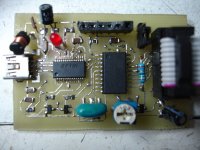
A small pcb has made with this technique.
The small i.c is FT232RL.
The small i.c is FT232RL.
Attachments
Last edited:
I found making my own pcbs very difficult.
One part of the pcb would be over etched while another part would be under etched.
I also found most of my projects were large doubled sided pc's.
So I gave up and used a pcb manufacturer.
I found the best and cheapest place was China.
I get pcb's in 2 weeks and have never had a bad pcb.
For home use a self made pcb sounds fine but I often sell on my stuff when I have used it a while and it needs to look pro with a proper solder resist and silk screen.
Who and HOW much? THanks
nice thread Mooly, i bought a samsung laser printer and is now starting to make boards....
Thanks 🙂
I also have a feeling that my UV tubes might be the incorrect wavelength. I usually need about 8-10 minutes of exposure which is a long way off the 3 minutes that Mooly suggests.
That is a long time. I just looked at the documentation with the lightbox and that recommends 2 to 2.5 minutes for Mega's own Foto Board and FPC-15 ? whatever that is.
I'm pretty sure that the Osram designation for the typical 15W 50cm tubes used in most lab UV boxes was TLA-15, but I'll have to check that.
If it means anything, mine are 8 Watt 05 12"
I use a high power SAD lamp to expose my boards, takes about 1 min 40 seconds. This helps a lot I think in creating good results.
That sounds quick but not a million miles away from Mega's light box.
One thing that is critical is the strength of the developer, erring on the side of caution and making it weaker than is recommended will prevent the photoresist from accidentally over-developing and stripping away. My boards often take around 5 minutes to develop with the advantage that I can actually leave the boards in the solution for a lot longer without it creating any issues too. When I had the developer stronger it would develop in 30 seconds to a minute, like they suggest, but I had to be extremely diligent in removing the board and washing it quickly, to make sure that things didn't go too far. This is far from optimal and even washing with hot water would cause a burst of developing where this water first hit and ruin a perfectly good board! So keep developer strength lower rather than higher and keep the rinse water cold.
Yep 😀 That was the first thing I found out the hard way. I watched the resist all dissolve away before my eyes. Good to know that you can go even weaker with the solution than the 18 to 1 that I recommended. Even at 18 to 1 a board develops in around 30 seconds I would say.
Thanks for the Wiki link too. Not had a chance to look yet but I will.
A small pcb has made with this technique.
The small i.c is FT232RL.
That looks good, SMD is always a challenge. I see you tinned all the traces on this one.
- Status
- Not open for further replies.
- Home
- Design & Build
- Construction Tips
- Making Perfect PCB's At Home.