Hi Chris ,the schematic shows no jumpers at all for any of the jumpers and it has many , J1302 I can only assume must be used to jump this spot in models that may not use this transistor because the jumper legs definitely terminate at 2 legs of the 2SD1266 transistor ( emitter & collector )and that can not be possible .. I do understand that not all components are installed in every model , what was throwing me was the jumper holes in J1302 had legs soldered into them that were cut off ,and as you can see in the picture quite a burn mark under the jumper symbol .. Maybe the guy goofed and installed a jumper thinking it was missing and that's what caused some of this damage . I did get a reply form another guy that worked on one of these recently and he did not seem to think it had anything in this spot . From what I'm seeing I'm going with empty as the verdict .. cheers
Yes, a previous repair "expert" may have installed a jumper that clearly was not originally installed. Who knows?
I need to have a look before I can answer you on this. I don't have time for that at the moment.
I need to have a look before I can answer you on this. I don't have time for that at the moment.
What a steep learning curve this hobby is , I've in 2 months built a basic lab and learned enough to get this old Luxman LV 105 going again .. looking forward to my next project . Many thanks to everyone that pitched in especially Anatech for his guidance .. cheers Roger

One thing is certain. That burnt part of the PCB is conducting = acts as a resistor/short.Ok guys having a bit of a problem here , I've been going through the circuit board repairing failed components and when I removed Q1301(transistor 2SD1266) to test it , don't even ask about the mangled holes.. I see beside it what I assume is a missing component , hard to read but looks like J1302 the board is showing the symbol for a jumper but when I look at the tracers on the back of the board the jumper would be jumping 2 legs of the transistor . is that even possible . The schematic does not show the placement of jumpers so I'm a bit in the dark as what to do here .. Anyone else with a LV105 that can confirm what if anything belongs in this spot would be extremely helpful , thanks so much guys ,Roger
You need to cut the burnt part off the PCB and rebuild the circuit off the PCB itself. Have seen this many times on various amps.
Even seen some PCB´s glowing when powered 😉
Hello Boydk,
Did you post in the wrong thread?
The unit is repaired and running. There was no charred PCB material noted - ever. The only times I have seen PCB conducting was under a couple of conditions.
If the issue is topical, you remove the material. Sometimes this is difficult as in the case of Adcom. Sometimes you have to buy a replacement PCB, or make one.
Nothing is ever certain unless you prove it by testing properly.
Did you post in the wrong thread?
The unit is repaired and running. There was no charred PCB material noted - ever. The only times I have seen PCB conducting was under a couple of conditions.
- Leaking electrolyte from those earlier problem capacitors.
- PCB material burned badly enough to create conductive carbon
- Degraded "glue" used to fix components to the PCB for wave soldering, dark brown to black means it could be conductive. Slightly conductive with lighter brown shades.
If the issue is topical, you remove the material. Sometimes this is difficult as in the case of Adcom. Sometimes you have to buy a replacement PCB, or make one.
Nothing is ever certain unless you prove it by testing properly.
Sorry, if I misunderstood something.Hello Boydk,
Did you post in the wrong thread?
I was referring to the picture in the quoted post #39
Well..... my limit for editing the post has expired, so feel free to do what you want with the post to clarify,Nope, you didn't miss anything, just the reference. I would clean that up.
or delete it all together, if it doesn´t make sense 😉
Just wanted to add a tidbit of information pertaining to the LV-105 (non ‘U’ version).
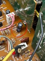
The pcb labeling for C1316 is reversed. Correct orientation is capacitor Negative leg facing the interior, Positive leg faces rear panel. The 1uF, 100V cap in the picture is toasted because it was installed following the pcb labeling.
This location has positive cap leg to ground, the schematic is correct.
Attachments
That's annoying, and I have seen it with many pieces of equipment. Sorry it bit you Vunce.
These days I take many pictures before I start. When replacing caps, I mark the negative side with a sharpie as well. Getting things in turned around because you followed the service manual shouldn't happen, but quality in manuals hit the skids in the 1980's too.
I don't trust anything.
These days I take many pictures before I start. When replacing caps, I mark the negative side with a sharpie as well. Getting things in turned around because you followed the service manual shouldn't happen, but quality in manuals hit the skids in the 1980's too.
I don't trust anything.
Yep, boy was I bitten by this one, in more ways than you’d think. Hehe.
I picked up this unit from a neighbor and it was in terrible condition! Even infested with cockroach's! 😳 (but that is a whole story within a story)
Anyway, once cleaned up and got a good look it needed many caps replaced, protection relay, pots and switches cleaned, corrosive glue removed and affected components plus Q1301.
When all was put back together the protection relay would engage after 20 seconds the disengage shortly afterwards. Hmmm, something is wonky. Thats when I found the bad cap. Checked the schematic for proper orientation and it was incorrect. But, taking many pictures, as I always do, before anything was touched is what saved my bacon. The original cap was installed correctly which looked incorrect by following the pcb labeling only.
Anatech, you are absolutely correct, don’t blindly trust the service manuals. So far every vintage component I’ve rehabbed has errors in the SM or pcb or both. (Yamaha B-2 had many issues)
The story has a good ending though, the LV-105 sounds great! Much better than expected. This is a keeper, pushing the AU-717 out of the rack. 😉
- Home
- Amplifiers
- Solid State
- Luxman LV105 need help