Congrats on this very cool project. I love the sound of the full sized amp and this with smaller inductors will make for an amazing preamp..dB
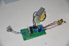
I'm going to try to use the Hammond 156C in my final build. It's small and not too expensive. I'll have to up the power supply voltage to about 60V, since the 156C's DC resistance is 3.7k ohms. The old Magnequest chokes that I've been testing are overkill. They're good for 60mA, and the circuit is only 8mA.
I replaced the big Magnequest inductor with a tiny Hammond 156C, dialed up the power supply to 60V, and ran some tests. I was pleasantly surprised to see that the Hammond is comparable to the Magnequest (distortion wise) in this situation. Not quite David versus Goliath, but nobody got hurt. I'd say it was a tie.
I adjusted the Lovoltech bias for best results and the resulting measurements are:
Power supply = 59.5V
MOSFET drain = 27.2V
Lovoltech drain = 4.56V
Lovoltech source = 1.60V (source resistor = 220 ohms)
Hammond 156C: 150H, 3.7k ohm DCR, rated at 8 mA
Depending on where you calculate the current (inductor or source resistor), quiescent current is approximately 8mA. Lovoltech Vds = 3.0V, Vgs = -1.6V.
The nice thing is I can buy a low VA Hammond power transformer with 2 x 60V secondaries for about $20 Canadian which would be perfect for a dual regulated power supply. Meanwhile, I can save the big, expensive Magnequest inductors for another project. And I can fit everything into a smaller case.
Attachments

I have been asked about making the Gerber files for the preamp PCB available. If you wish a copy, send me a mail and I will send you a zip file containing the Gerbers. I will also make the power supply regulator PCB available after I have received and tested it.
Nice Preamp project Pinholer!
The LU1014D aluminum adapter board is perfect for an all in one mounting/heatsink solution👍
The LU1014D aluminum adapter board is perfect for an all in one mounting/heatsink solution👍
Thanks, Vunce. Before I discovered the LU1014D, I didn't even know that there were aluminum PCBs.
Google "aluminum pcb substrate". There are lots of references. There's an aluminum base layer, a dielectric layer, and then the copper layer. The copper is etched for surface mount devices. The PCB can be attached to a heatsink to carry heat away.
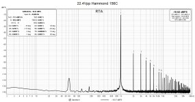
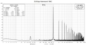
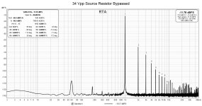
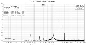
I've been working in LTspice exploring the the characteristics of this preamp circuit with the Hammond 156C inductor. The higher inductance (150 H) has increased the gain so I increased the negative feedback in the simulation. One thing lead to another and I modeled the output impedance. Alas, it came out to over 2k ohms. That was high enough to concern me.
After studying the circuit a bit, I realized that the unbypassed source resistor (220 ohms) would contribute to the higher output impedance. A solution, then, would be to add a bypass capacitor. With the source resistor bypassed, LTspice calculates output impedance of about 140 ohms in the audio frequencies.
With the source resistor bypassed, the gain goes up as the local negative feedback is removed. I increased the global negative feedback to bring the gain back to about 9.
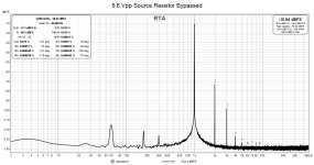
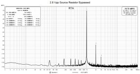
I made the changes to the prototype and ran some tests. Overall gain was about 8.5. The output impedance at 1 kHz came out at about 155 ohms. So, LTspice was close. And I'm happy about the output impedance.
I reran the distortion tests at various output levels. The total harmonic distortion numbers increased, more at lower levels than at high outputs. At 1 Vrms out, the THD increased about 3 times compared to prior tests, from 0.004% to 0.012%. At high output levels, the differences were much less.
One aspect about the harmonic distortion results that changed in the positive direction was the distortion profile. The results with the bypassed source resistor contains significantly lower higher order distortion products. The harmonic distortion profile decreases more smoothly as the harmonics increase.
In the end, I think the higher total harmonic distortion numbers are worth the lowered output impedance and the nicer harmonic distortion profile.
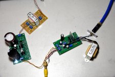
The regulated power supply PCBs have arrived, as well as some parts from DigiKey, so the next step is to assemble the power supply and test it.
After studying the circuit a bit, I realized that the unbypassed source resistor (220 ohms) would contribute to the higher output impedance. A solution, then, would be to add a bypass capacitor. With the source resistor bypassed, LTspice calculates output impedance of about 140 ohms in the audio frequencies.
With the source resistor bypassed, the gain goes up as the local negative feedback is removed. I increased the global negative feedback to bring the gain back to about 9.
I made the changes to the prototype and ran some tests. Overall gain was about 8.5. The output impedance at 1 kHz came out at about 155 ohms. So, LTspice was close. And I'm happy about the output impedance.
I reran the distortion tests at various output levels. The total harmonic distortion numbers increased, more at lower levels than at high outputs. At 1 Vrms out, the THD increased about 3 times compared to prior tests, from 0.004% to 0.012%. At high output levels, the differences were much less.
One aspect about the harmonic distortion results that changed in the positive direction was the distortion profile. The results with the bypassed source resistor contains significantly lower higher order distortion products. The harmonic distortion profile decreases more smoothly as the harmonics increase.
In the end, I think the higher total harmonic distortion numbers are worth the lowered output impedance and the nicer harmonic distortion profile.
The regulated power supply PCBs have arrived, as well as some parts from DigiKey, so the next step is to assemble the power supply and test it.
Attachments

Before I saw your post I was wondering if the Bride of Zen could be
modified to be like your circuite. But I was woried that the Ld1014d
might have a lot of noise and distortion when used at a relativly low
current but you are geting excelent results. Did you look at the noise
and distortion when biased a little higher or running a 2 of the Ld1014
in parallel ?
modified to be like your circuite. But I was woried that the Ld1014d
might have a lot of noise and distortion when used at a relativly low
current but you are geting excelent results. Did you look at the noise
and distortion when biased a little higher or running a 2 of the Ld1014
in parallel ?
With a current of 11 mA, you might try substituting the big mosfet for a little bjt, like the bc550 or ksc1845. Might improve the sound.
When I had my big Magnequest choke (designed for 60 mA) in place as the load, I experimented with various source resistances to change Vgs and found that around 11 mA with Vds of approximately 3.2V was the sweet spot for minimum distortion.
In terms of trying smaller MOSFET or BJT as the amplifying device, I have modeled that in LTspice and there is not much difference. Of course, reality may be different. I need to try that.
There is variation among the Lovoltechs in measured characteristic curves, so I think by far, the most significant changes can be made by using a different LU1014D. Optimizing the circuit for one specific Lovoltech in the prototype may result in disapointment when building the final circuits with different Lovoltechs.
Having said that, the next thing that I will try, though, is to up the power supply voltage. So far, in my experiments, higher power supply voltage lowers distortion. My lab power supply maxes out a 60V so that is what I have used so far. I have a 60V transformer that may be able to provide up to 75V of regulated power, so I will see what happens with a higher power supply. I will do that once I have built and tested my regulated PS.
On the F3, the optimal value for the Source resistor was based on the Vp or Idss of the
Jfet, and through testing a population a graphic was made of that value. After that, on
a given channel the Gate voltage of the Cascode was adjusted by the pot to set the Vds
of the Jfet. Given this it becomes easy to get consistent results and the pot can then be
adjusted for a specific harmonic profile or least distortion.
Over the last two days, I populated the regulated power supply board. Along the way, I found a couple of problems. Not show stoppers, but not ideal.
First, I had the wrong footprint for the bridge rectifier. I had to drill two new holes and then bend the legs so they touched the pads.
The second problem was that my main input filter capacitor was larger diameter than the footprint that I chose. Originally, I had planned to use 80V capacitors, but after ordering the PCBs, I thought it would be prudent to use 100V rating instead. The result is a tight fit. It works for this test PCB, but for the final build with the snubber components to be installed, some creative parts placement may be necessary. I will make revisions to the PCB.
I decided that for this test power supply, I would aim for 75 volts out. I installed 4 x 15V zeners and 2 x 9.1V zeners for a total of about 78V at the gate of the MOSFET follower. That combined with its Vgs of about 5V should give a regulated output of about 73V.
The Hammond power transformer that I bought has 115V primary and 2 x 60V secondaries. The local line voltage is around 120V and can be higher at times. I did some measurements at mid-day today and found the line voltage at 120.0VAC and the secondary at 69.9VAC.
DC voltage after the input filter capacitor came to 88.0V (why I ordered 100V capacitors) and the final regulated output was 73.2V. So, the power supply PCB is working correctly, albeit with some footprint issues.
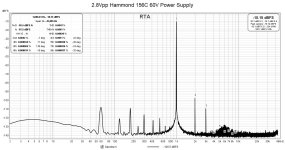
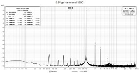
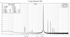
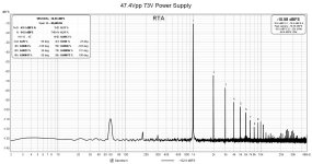
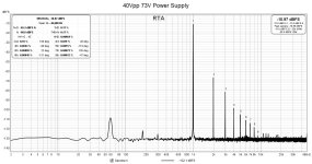
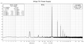
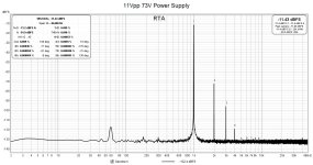
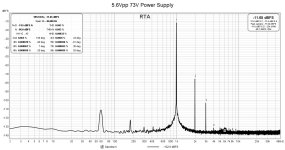
I connected the power supply to the preamp board and conducted some distortion tests. The harmonic distortion at 2.8Vpp (1V RMS) is basically the same as with the 60V power supply. At higher output voltages, the harmonic distortion profiles start looking better than those using the 60V power supply.
This results in an increase in output voltage for the same total harmonic distortion. The distortion at 47.4Vpp out with the 73V power supply is lower than that of the 34Vpp output with the 60V power supply.
Increasing the power supply voltage is a good idea if high voltage output is needed. The extra cost basically comes down to higher voltage electrolytic capacitors. The power transformer VA requirement is quite low, so that doesn't affect the cost much.
First, I had the wrong footprint for the bridge rectifier. I had to drill two new holes and then bend the legs so they touched the pads.
The second problem was that my main input filter capacitor was larger diameter than the footprint that I chose. Originally, I had planned to use 80V capacitors, but after ordering the PCBs, I thought it would be prudent to use 100V rating instead. The result is a tight fit. It works for this test PCB, but for the final build with the snubber components to be installed, some creative parts placement may be necessary. I will make revisions to the PCB.
I decided that for this test power supply, I would aim for 75 volts out. I installed 4 x 15V zeners and 2 x 9.1V zeners for a total of about 78V at the gate of the MOSFET follower. That combined with its Vgs of about 5V should give a regulated output of about 73V.
The Hammond power transformer that I bought has 115V primary and 2 x 60V secondaries. The local line voltage is around 120V and can be higher at times. I did some measurements at mid-day today and found the line voltage at 120.0VAC and the secondary at 69.9VAC.
DC voltage after the input filter capacitor came to 88.0V (why I ordered 100V capacitors) and the final regulated output was 73.2V. So, the power supply PCB is working correctly, albeit with some footprint issues.
I connected the power supply to the preamp board and conducted some distortion tests. The harmonic distortion at 2.8Vpp (1V RMS) is basically the same as with the 60V power supply. At higher output voltages, the harmonic distortion profiles start looking better than those using the 60V power supply.
This results in an increase in output voltage for the same total harmonic distortion. The distortion at 47.4Vpp out with the 73V power supply is lower than that of the 34Vpp output with the 60V power supply.
Increasing the power supply voltage is a good idea if high voltage output is needed. The extra cost basically comes down to higher voltage electrolytic capacitors. The power transformer VA requirement is quite low, so that doesn't affect the cost much.
Attachments

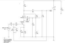
Here is the list of components for the preamp PCB:
M1 IRFP240N
T1 LU1014D (assumes 200 ohm gate resistor on PCB)
D1 12V Zener Diode
J2 Hammond 156C, 150H, 3700 ohms
C1 100uF 100V (voltage rating depends on power supply voltage)
C2 10uF 50V output capacitor
C3 output bypass capacitor 50V, 10mm lead spacing
C4 220uF 15V
C5 20pF
R4 2200uF 10V *note - place bypass capacitor here instead of resistor
R1 47.5k
R2 200
R3 220 may be adjusted for lowest distortion
R5 20k trimmer pot, Bourns PV36W203C01B00, inline 2.54mm pitch
R6 20k
R7 5k negative feedback resistor.........
A few of notes:
- C1, the power supply decoupling capacitor is sized according to the power supply voltage. I am using a 73V power supply so I have chosen a 100V capacitor.
- R3, the JFET source resistor, can be adjusted for lowest output distortion. 200 ohms is a good starting point.
- R4 was originally intended to be used to adjust the JFET source resistance by paralleling with R3. I have used it instead to insert a bypass capacitor.
- J2 is used for the load. I am using an Hammond inductor. Other loads, such as a resistor, may be used instead. For example, you could replace the Hammond inductor with a 3700 ohm resistor. This works well for lower output voltages, but distortion increases at higher outputs.
- depending on whether you want to use global negative feedback or not, place jumper in J5 or J6. R7 may be replaced with a jumper if no feedback is chosen.
Attachments

I'm still working on this project, although on a bit of a sidetrack. I want to use matched pairs of JFETs for my stereo preamp and my yet-to-be finished common source Lovoltech power amp, and I have no more matched sets of LD1014Ds. However, I have over thirty LD1014Ds waiting to be soldered onto aluminum PCBs and I've not been eager to embark on this task with my fry pan on the stove top.
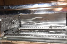
Coincidently, about two weeks ago, I read an article on hackaday.com about a DIY Arduino controlled reflow hotplate project. This got me thinking and after more research, I decided that I would build an Arduino controlled reflow toaster oven. It just happens that I have an unused toaster oven that's been sitting around for probably 20 years.
From my research, I learned that heating capacity is important, and a quick test with a thermocouple revealed that this oven takes about 3 minutes to reach an interior temperature of about 230 degrees Celsius. This works out to be just over 1 deg. C / second. The recommended minimum heating rate is around 2 deg. C / second. I figured that if I added insulation to the oven walls, I could meet that target.
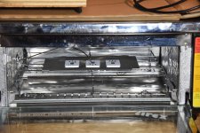
I took apart the oven, removed all the electrical controls, and hardwired the four heating elements directly to the power cord. Then, I added pink fibreglass insulation and thin aluminum sheeting to all the interior surfaces except for the front door. A K type thermocouple was installed through the side for temperature monitoring.
With the insulation added, it took only about 90 seconds for the oven to reach 230 degrees C (over 2 deg. C / second). Uninsulated, it had taken 3 minutes, or twice as long. I had been debating about whether I should insulate the door, but given the great improvement already achieved, I decided that I would proceed with the oven as is, at least for now.
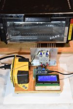
I found from my online reseearch that there is an Arduino reflow controller by Rocket Scream which is quite popular (must be good!). Rocket Scream makes available the Arduino code for people to use, so I took advantage of that. I assembled my own controller hardware and modified the Arduino code for my configuration and after making sure everything was working properly, I proceeded to tune the controller PID variables.
It did not take too many iterations before I managed to produce a heating profile that looks to be useable for leaded solder paste. The controller does all the work until maximum temperature is reached, and then I manually open the door slowly to manage the cool-down.
Before I start using this oven for real, I will place an old circuit board in the oven with the thermocouple touching its surface and see how the heating profile turns out with an actual PCB. The tests so far have just been measuring the interior air temperature.
If all goes well, I may actually enjoy soldering the rest of the LD1014Ds.
Coincidently, about two weeks ago, I read an article on hackaday.com about a DIY Arduino controlled reflow hotplate project. This got me thinking and after more research, I decided that I would build an Arduino controlled reflow toaster oven. It just happens that I have an unused toaster oven that's been sitting around for probably 20 years.
From my research, I learned that heating capacity is important, and a quick test with a thermocouple revealed that this oven takes about 3 minutes to reach an interior temperature of about 230 degrees Celsius. This works out to be just over 1 deg. C / second. The recommended minimum heating rate is around 2 deg. C / second. I figured that if I added insulation to the oven walls, I could meet that target.
I took apart the oven, removed all the electrical controls, and hardwired the four heating elements directly to the power cord. Then, I added pink fibreglass insulation and thin aluminum sheeting to all the interior surfaces except for the front door. A K type thermocouple was installed through the side for temperature monitoring.
With the insulation added, it took only about 90 seconds for the oven to reach 230 degrees C (over 2 deg. C / second). Uninsulated, it had taken 3 minutes, or twice as long. I had been debating about whether I should insulate the door, but given the great improvement already achieved, I decided that I would proceed with the oven as is, at least for now.
I found from my online reseearch that there is an Arduino reflow controller by Rocket Scream which is quite popular (must be good!). Rocket Scream makes available the Arduino code for people to use, so I took advantage of that. I assembled my own controller hardware and modified the Arduino code for my configuration and after making sure everything was working properly, I proceeded to tune the controller PID variables.
It did not take too many iterations before I managed to produce a heating profile that looks to be useable for leaded solder paste. The controller does all the work until maximum temperature is reached, and then I manually open the door slowly to manage the cool-down.
Before I start using this oven for real, I will place an old circuit board in the oven with the thermocouple touching its surface and see how the heating profile turns out with an actual PCB. The tests so far have just been measuring the interior air temperature.
If all goes well, I may actually enjoy soldering the rest of the LD1014Ds.
Attachments
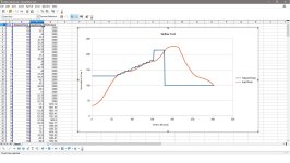

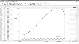

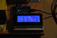
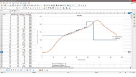
I made some modifications to the Arduino code so I could better follow the reflow process without monitoring the data on another computer through a serial port. The reflow controller LCD has 4 lines so I added display of elapsed times when temperature is above 183 C, when temperature is above 215 C; the maximum temperature reached; and the heating / cooling rate.
I have found recommendations for keeping the time above 183 C to 50 - 80 seconds and maximum of 30 seconds above 215 C. Also, the maximum cooling rate should be no more than 4 C/sec.
After the reflow controller has completed its heating cycle, I keep an eye on the elapsed time above 215 C, and when that reaches about 15 seconds, I open the door a little to start the rapid cooling process. I then gradually keep opening the door until it is fully open. I can adjust the cooling rate with some fanning action.
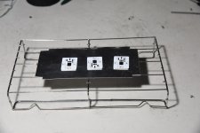
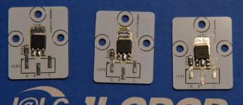
Today, I did the first real reflow. I started out with a single LU1014D aluminum PCB and two unpopulated PCBs on the oven rack. I had load tested the oven yesterday with just unpopulated PCBs and the temperature profiles were good, so I was confident that it would work. The finished board looked good and ohmmeter checks passed. The first PCB was a successen, I did a batch of two more PCBs and that completed my first reflow session with the oven.
Overall, I'm very happy with the results. After my internet research, it appeared that getting an acceptable reflow heating profile with a DIY toaster oven was hit and miss. I think that I was lucky that my toaster oven has good heat capacity which allowed reasonable heating rates. I'm also impressed with the PID temperature control. I've tested the reflow procedure many times now and the repeatability is very good. Way better than my manually controlled stove element heating a fry pan.
I've been avoiding reflowing the Lovoltechs onto the aluminum PCBs but, now, with this reflow oven, it might even be fun.
I have found recommendations for keeping the time above 183 C to 50 - 80 seconds and maximum of 30 seconds above 215 C. Also, the maximum cooling rate should be no more than 4 C/sec.
After the reflow controller has completed its heating cycle, I keep an eye on the elapsed time above 215 C, and when that reaches about 15 seconds, I open the door a little to start the rapid cooling process. I then gradually keep opening the door until it is fully open. I can adjust the cooling rate with some fanning action.
Today, I did the first real reflow. I started out with a single LU1014D aluminum PCB and two unpopulated PCBs on the oven rack. I had load tested the oven yesterday with just unpopulated PCBs and the temperature profiles were good, so I was confident that it would work. The finished board looked good and ohmmeter checks passed. The first PCB was a successen, I did a batch of two more PCBs and that completed my first reflow session with the oven.
Overall, I'm very happy with the results. After my internet research, it appeared that getting an acceptable reflow heating profile with a DIY toaster oven was hit and miss. I think that I was lucky that my toaster oven has good heat capacity which allowed reasonable heating rates. I'm also impressed with the PID temperature control. I've tested the reflow procedure many times now and the repeatability is very good. Way better than my manually controlled stove element heating a fry pan.
I've been avoiding reflowing the Lovoltechs onto the aluminum PCBs but, now, with this reflow oven, it might even be fun.
Attachments
- Home
- Amplifiers
- Pass Labs
- LU1014D Preamp