Hi all,
I performed a search on the forum but I found no clear thread to teach a newbie like me how to simulate PSRR of a discrete voltage regulator in LTSpice.
Can someone be so kind to post some simple steps in order to simulate and plot PSRR of a discrete voltage regulator in LTSpice (or, at least, provide a link...)??
Many thanks
Dan
Does "item 9" in the index here help ?
http://www.diyaudio.com/forums/software-tools/260627-installing-using-ltspice-beginner-advanced.html
http://www.diyaudio.com/forums/software-tools/260627-installing-using-ltspice-beginner-advanced.html
Yes! I read it and oh, thank you very much for that Mooly!!!!! I got the first information on simulating with LTSpice.
But, once I have the ripple on Vin and Vout what should I plot?
I suppose something like 20*log(Vout / Vin) on the y axis and frequency on the x axis. Right?
But, once I have the ripple on Vin and Vout what should I plot?
I suppose something like 20*log(Vout / Vin) on the y axis and frequency on the x axis. Right?
I see what you mean... yes 20log and so on, but how do manufacturers derive a figure I wonder. Would they apply a regular symmetrical ripple (such as a sine) at a specific frequency and work out a value from that. I suppose you could work out a figure taking peak values... I honestly don't know.
I think to compare figures of a diy build to say a 78xx then you need to have the same ripple conditions. There must be some industry standard I would have thought.
I think to compare figures of a diy build to say a 78xx then you need to have the same ripple conditions. There must be some industry standard I would have thought.
And what about the strange behavior when, sometimes, LTSpice shows: "Stepping Source" and starts with strange calculations that never end? Sometimes I cannot simulate a circuit due to this behavior....
Thanks!!!
Thanks!!!
Just a guess but you you might be able to stop that by adding something seemingly irrelevant such as a 10meg across some part of the circuit. I've occasionally encountered something similar.
If that doesn't work then post the .asc file and we'll take a look.
If that doesn't work then post the .asc file and we'll take a look.
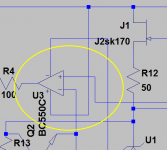
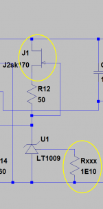
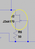
Got the file 🙂 but your going to have to help me out on this...
It opens with no symbol for the MAX chip, and I can't find your models for the BC550 and 560
It opens with no symbol for the MAX chip, and I can't find your models for the BC550 and 560
I made a few quick changes to the schematic and it simulated just fine on a Windows7 PC
- Interchange M2's source and drain
- Interchange J2's source and drain
- Interchange J1's source and drain
- Connect infinity ohm resistor to U1's trim pin
- Replace Maxim opamp model with UniversalOpamp2 because the Maxim's Symbol was not included in the .zip file
Attachments

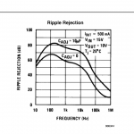
The poor low frequency behaviour must be thermal, which simulators like LTSpice usually ignoreFrom an LM317 data sheet so it seems from this that they must apply a known fixed (sine ???) type ripple.
Hi guys,
Thank you very, very, much for your help!
I will try a prototype this week!
BTW I will try an AD797 jewelry-opamp. Does it work single supply?
I also find an Intersil ultra low noise reference I would like to try: http://www.intersil.com/content/dam/Intersil/documents/isl2/isl21090.pdf
I am also thinking about using a BJT as shunt element for better regulation.
Dan
Last edited:
The AD797 will work on single rail for something like this but it seems a waste tbh.
I say this every time with regs... its one thing having an ideal low noise voltage source... quite another keeping that way at its destination.
You need to back up the simulations with a real build under real world conditions too.
I say this every time with regs... its one thing having an ideal low noise voltage source... quite another keeping that way at its destination.
You need to back up the simulations with a real build under real world conditions too.
The most difficult part for a DIYer is performing a current set of tests on prototypes. In my next life, or if the devil wants to buy my soul, I will buy an AP x52x audio analyzer.
Currently I am looking for a decent condition system one. But I it is difficult to source good condition one, actually.
Now I need to plan a test set using an Agilent DSO2004A scope and a Tek DM4040 multimeter lol.
Back to the reg, in order to keep this as low noise as possible at the destination, I am planning to build it on the same board that has DAC section in order to have no wire from the supply to the target device.
I have a Naim CDX, good stuff, and I bought also its external XPS supply. It improved the performances a lot but, if you open it, you would be surprized to find that it contains a cascade of quite cheap regulators. So my guess is that low noise layout goes far than the components and topology used lol.
Dan
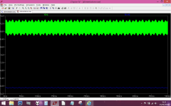
Testing isn't always easy but you should do basic tests, even if its just using a wideband scope. There are different aspects to reg design, low noise just being one of them. How the reg behaves under transient load conditions is important too.

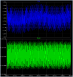
It looks excellent judging by the peak amplitudes. What current is the pulsed source pulling from the supply ?
It will be interesting to see how a real build compares.
It will be interesting to see how a real build compares.
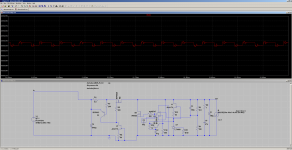
Installing a 50pF capacitor to the compensation/decoupling pin of the AD797, as suggested by the DS, further improves the performances.
About the current from the supply, it is pulling 116mA. 70mA are "wasted" in the shunt element, 4mA biasing the CCS, 8mA in the feedback divider, 4mA in the LT1006 (it will be reduced in the prototype), 3mA for the capacity multiplier the other for opa supply. 😎
About the current from the supply, it is pulling 116mA. 70mA are "wasted" in the shunt element, 4mA biasing the CCS, 8mA in the feedback divider, 4mA in the LT1006 (it will be reduced in the prototype), 3mA for the capacity multiplier the other for opa supply. 😎
Attachments
- Status
- Not open for further replies.
- Home
- Design & Build
- Software Tools
- LTSpice and discrete regulator PSRR