Would it be possible to get 4 Vrms output instead of 0,6 Vrms?
If so, how?
/S
If so, how?
/S
Nope ... should be around 600mV rms.
It is designed to be like that because my RMI-FC100 amp allow only 600mVpp at input for full output power.
Would it be possible to get 4 Vrms output instead of 0,6 Vrms?
If so, how?
/S
Why do you need that?
The distortion will be higher for 15V Vcc, power dissipation also if you will be forced to increase Vcc in order to keep the same THD spectrum.
I use a line amp in between the IV converter and the power amp. And all my gear follow the standard output voltage, ie 2Vrms single ended and 4Vrms balanced. Makes life so much easier. Having only 0,6Vrms is far to low.
Some extra heat is fine, and a higher rails is OK. I often use 24 - 36VDC myself.
With this in mind, how would you change your design to get 4Vrms output voltage?
/S
Some extra heat is fine, and a higher rails is OK. I often use 24 - 36VDC myself.
With this in mind, how would you change your design to get 4Vrms output voltage?
/S
Why do you need that?
The distortion will be higher for 15V Vcc, power dissipation also if you will be forced to increase Vcc in order to keep the same THD spectrum.
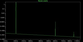
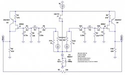
This are the results for 4V rms analog output at 0dB digital output.
The power supply voltage was increased at 30Vdc, hence R7 and R10 dissipates now around 1W, Q1 and Q2 dissipates 250mW and were upgraded to 2sa1360 (must be placed on a small heatsink)
You need to supply a very clean power voltage, preferably from a shunt regulator capable to give 30V/150mA per each channel.
Fourier components of V(vout-,vout+)
DC component:-0.00077357
Harmonic Frequency Fourier Normalized Phase Normalized
Number [Hz] Component Component [degree] Phase [deg]
1 2.000e+04 5.532e+00 1.000e+00 -1.61° 0.00°
2 4.000e+04 1.170e-07 2.115e-08 179.69° 181.30°
3 6.000e+04 1.199e-04 2.167e-05 42.36° 43.96°
4 8.000e+04 6.279e-08 1.135e-08 -177.48° -175.87°
5 1.000e+05 5.828e-07 1.054e-07 -124.63° -123.03°
6 1.200e+05 3.940e-08 7.122e-09 176.83° 178.44°
7 1.400e+05 2.358e-08 4.262e-09 173.40° 175.01°
8 1.600e+05 2.870e-08 5.189e-09 177.14° 178.75°
9 1.800e+05 4.302e-08 7.777e-09 172.44° 174.04°
Total Harmonic Distortion: 0.002168%
Attachments
Last edited:
Thank you!
God work getting very low THD with this output voltage, too!
I am doing the simulation now. May I ask what currents go through
R8
R10
R11
?
Kind regards,
S
God work getting very low THD with this output voltage, too!
I am doing the simulation now. May I ask what currents go through
R8
R10
R11
?
Kind regards,
S
This are the results for 4V rms analog output at 0dB digital output.
The power supply voltage was increased at 30Vdc, hence R7 and R10 dissipates now around 1W, Q1 and Q2 dissipates 250mW and were upgraded to 2sa1360 (must be placed on a small heatsink)
You need to supply a very clean power voltage, preferably from a shunt regulator capable to give 30V/150mA per each channel.
Fourier components of V(vout-,vout+)
DC component:-0.00077357
Harmonic Frequency Fourier Normalized Phase Normalized
Number [Hz] Component Component [degree] Phase [deg]
1 2.000e+04 5.532e+00 1.000e+00 -1.61° 0.00°
2 4.000e+04 1.170e-07 2.115e-08 179.69° 181.30°
3 6.000e+04 1.199e-04 2.167e-05 42.36° 43.96°
4 8.000e+04 6.279e-08 1.135e-08 -177.48° -175.87°
5 1.000e+05 5.828e-07 1.054e-07 -124.63° -123.03°
6 1.200e+05 3.940e-08 7.122e-09 176.83° 178.44°
7 1.400e+05 2.358e-08 4.262e-09 173.40° 175.01°
8 1.600e+05 2.870e-08 5.189e-09 177.14° 178.75°
9 1.800e+05 4.302e-08 7.777e-09 172.44° 174.04°
Total Harmonic Distortion: 0.002168%
Please find below the requested values:
I(R8 = 5.14 / 5.19mA
I(R10) = 48.7 / 56.8mA
I(R11) = 10.26 / 12.7mA
The above min and max values are for full output swing.
I(R8 = 5.14 / 5.19mA
I(R10) = 48.7 / 56.8mA
I(R11) = 10.26 / 12.7mA
The above min and max values are for full output swing.
Thanks, roender!
To get 4,0Vrms output, and have the currents you wrote down, I had to change a resistor value into half what you suggested, and I had to increase the 1k1 into 1k75.
THD is about -88 dB in balanced mode as the even order harmonics cancel out. In the real world, where an amplifier does the balanced to single ended conversion, even order harmonics will not cancel out as well.
In SE mode, THD is rather high at -61 dB simulating at 1kHz and 2Vrms out at 0 dBFS (16mAACp-p).
See attachments.
/S
Please find below the requested values:
I(R8 = 5.14 / 5.19mA
I(R10) = 48.7 / 56.8mA
I(R11) = 10.26 / 12.7mA
The above min and max values are for full output swing.
Attachments
If you are using Buffalo II or III DAC the output current is actually 17.2mA pp.
Better use the same source as in my simulation, a voltage source with 1.715V DC offset and 1.69V swing at 0dB output followed by 195ohm series resistor.
Better use the same source as in my simulation, a voltage source with 1.715V DC offset and 1.69V swing at 0dB output followed by 195ohm series resistor.
I should haev told you about my source. It uses 195.3128 resisors which are inseries with the sine generator, and also in series are 1,65VDC batteries. I use an inverter so that only one sine source is used.
So, we are using the same system except that I use the (recommended) 3V3 instead of Twisted Pears 3V5.
What single ended THD do you get with 4,0Vrms output voltage?
/S
So, we are using the same system except that I use the (recommended) 3V3 instead of Twisted Pears 3V5.
What single ended THD do you get with 4,0Vrms output voltage?
/S
If you are using Buffalo II or III DAC the output current is actually 17.2mA pp.
Better use the same source as in my simulation, a voltage source with 1.715V DC offset and 1.69V swing at 0dB output followed by 195ohm series resistor.
I should haev told you about my source. It uses 195.3128 resisors which are inseries with the sine generator, and also in series are 1,65VDC batteries. I use an inverter so that only one sine source is used.
So, we are using the same system except that I use the (recommended) 3V3 instead of Twisted Pears 3V5.
What single ended THD do you get with 4,0Vrms output voltage?
/S
Do you mean 2V rms single ended, because 4V rms is pointless for a single ended preamplifier?!

I get -59 dB THD20k at 2Vrms output voltage which is about 20 dB worse than you get. I have tried the design with both your values for the 4V version, and also with my values. You vales give me only 3,6Vrms (balanced, 1.8Vrms single ended) using 16 mAACp-p signal input.
Not sure what the discrepancy is caused by.Might be the models.
Did you even consider making a DC coupled version by foloding down the entire schematic and making a complementary version?
/S
Not sure what the discrepancy is caused by.Might be the models.
Did you even consider making a DC coupled version by foloding down the entire schematic and making a complementary version?
/S
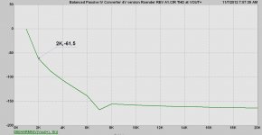
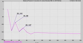
SE analog output at 2Vrms (0dB digital), THD 20kHz
Member
Joined 2006
I understand your latest output stage has evolved into the one below.
http://www.diyaudio.com/forums/digital-line-level/117238-ess-sabre-reference-dac-8-channel-246.html
So you now prefer it in voltage mode with higher output that gets filtered before going to a unity gain buffer while previously you had it in a sort of forced current mode then to a microphone preamp...
Could you describe the sonic differences? Is the filtering very important?
And would it be even neater to implement a common mode filter going into the buffers? Thanks roender.
Attachments
- Status
- Not open for further replies.
- Home
- Source & Line
- Digital Source
- Low distortion, pure resistive I/V stage for Sabre Reference DAC