Wich Idss for 170s & for 117s? Sorry my ignorance inputs are V2 & V3, right? Is powered only with +15VDC?
Should be BL grade each of them.
V2 and V3 plus R12 and R13 are inside of Sabre DAC ;-)
I also think that a simple but good circuit has the potential to sound very good. Is now post 18 the favorite ?
The post 18 contains the final solution for IV stage.
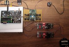
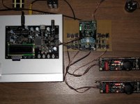
I'm done with the transport. I have found Nirvana 🙂 which is SDtrans384 plus Sabre Reference DAC in sync mode with the transport. SDtrans now generates the MCLK for the DAC but in the future it ewill be a dual clock board tided closely to the DAC and it will send back to the transport the required clock for the played source file, standard or high resolution PCM.
Attachments
Hi roender,
May I ask where you purchased your SD transport?
Ask Bunpei member.
Cheers
Felipe
get ready for $$$$ =) Ryan. sdtrans is very nice, but the price is high due to small runs and high quality parts
btw interesting circuit, does AVCC/2 play a part for gate bias? I cannot tell if R14/R19 are connected across actual ground, or across AVCC. IV resistors are increased to 2r2? I ask because I have some very nice TX220 texas components sfoil in 0.5% 0r66 that I could combine to make for 0r99 easily enough.
sk369 could be interesting here too, I have some matched, high gM quads
Last edited:
get ready for $$$$ =) Ryan. sdtrans is very nice, but the price is high due to small runs and high quality parts
btw interesting circuit, does AVCC/2 play a part for gate bias? I cannot tell if R14/R19 are connected across actual ground, or across AVCC. IV resistors are increased to 2r2? I ask because I have some very nice TX220 texas components sfoil in 0.5% 0r66 that I could combine to make for 0r99 easily enough.
sk369 could be interesting here too, I have some matched, high gM quads
The offset voltage generated by the DAC do not mater. R14/19 are connected from the output of the DAC to ground.
This I/V stage can be seen as a microphone amplifier. The input resistor was increased to 2r2 in order to improve SNR to more than 125dB over 10-20kHz bandwidth. The Sabre Reference DAC is working now in "voltage mode" ... but is a voltage DAC anyway no mater what ESS is telling 😛
get ready for $$$$ =) Ryan. sdtrans is very nice, but the price is high due to small runs and high quality parts
Yes, as i just recently discovered 😱, i think ill stick with the cheap QA550 for now.🙂
No, it isn't. It was just for simulation. The only load seen by the I/V stage is the 22k volume attenuator located into the power amplifier.
Guys, as far as I listened, this is the best sounding I/V stage I have tested. And i had listened many.
It is very simple to construct, just be sure that jfets are sorted to the same Idss in every similar symmetrically position
Hi Roender, compliments ,have you listened the Sen I/V of Patrick EUVL also?
I don't understood how you connect the Buffalo to I/V converter.
I think you connect Iout+ of BIII to J1 gate, the Iout- to J2 gate and the 2.2 resistors between the gates and out ground of BIII. I'm right?
Why some resistors have strange values (235 ,360 and 80 Ohm)? Are these values mandatory? Please let me know. Thanks in advance.
Best, Orazio
Hi Orazio,
I had listened to many I/V stages but I do not wanna give names and subjectively review them.
You are correct regarding how to connect analog outputs of the DAC to the I/V converter.
Now, regarding resistors, 80 ohms is just in simulation in order to get the same current value as the one in real life. Instead of resistors value I will post a schematic with currents for every stage.
Stay tuned.
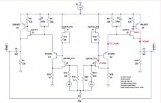
I'm not experienced like you, but I think the resistor values depending from the Idss of Jfets and hfe of BJTs to give the current that you want. For example the 2.5mA that polarize J1 and J2 are feed by CCS formed by J6 and J7 and R16 and R17. Right?
And 2.5mA depending by Idss and resistor value.
What's the Vout RMS in balanced mode? Of course with BIII?
Thanks for the quick reply.
Best, Orazio
And 2.5mA depending by Idss and resistor value.
What's the Vout RMS in balanced mode? Of course with BIII?
Thanks for the quick reply.
Best, Orazio
You are correct in your assumptions related with biasing currents for CFP Njfet driver. In fact, you can choose jfets with 2.5mA idss and then not need any resistor for CCS current setting.
Vout[rms] = 650mV
Vout[rms] = 650mV
How about raising the ground reference to AVCC/2 to be compliant?
The offset voltage generated by the DAC do not mater. R14/19 are connected from the output of the DAC to ground.
This I/V stage can be seen as a microphone amplifier. The input resistor was increased to 2r2 in order to improve SNR to more than 125dB over 10-20kHz bandwidth. The Sabre Reference DAC is working now in "voltage mode" ... but is a voltage DAC anyway no mater what ESS is telling 😛
How about raising the ground reference to AVCC/2 to be compliant?
Would you please be more specific? Compliant with what?
What can be gained by rising the DAC output return to a steady potential of AVCC/2 than ground?
Nice IV converter!
I "hooked" it up in MicroCap10 Pro, and I have some issues with the lowish output voltage. It is ,when an ESS9018 is outputtting 16mA ACp-p + 8mA DC, only 0.4Vrms instead of the standardised 4 Vrms.
Do you also get 0,4Vrms at 0 dBFS?
/S
I "hooked" it up in MicroCap10 Pro, and I have some issues with the lowish output voltage. It is ,when an ESS9018 is outputtting 16mA ACp-p + 8mA DC, only 0.4Vrms instead of the standardised 4 Vrms.
Do you also get 0,4Vrms at 0 dBFS?
/S
Schematic
Seems strange to me, too.
That would mean that the ESS9018 would not output any DC current (only AC current), right?
/S
That would mean that the ESS9018 would not output any DC current (only AC current), right?
/S
Would you please be more specific? Compliant with what?
What can be gained by rising the DAC output return to a steady potential of AVCC/2 than ground?
Seems strange to me, too.
That would mean that the ESS9018 would not output any DC current (only AC current), right?
/S
I know what will happens if the output reference will be avcc/2, but is not clear what benefit will bring that.
Nice IV converter!
Do you also get 0,4Vrms at 0 dBFS?
/S
Nope ... should be around 600mV rms.
It is designed to be like that because my RMI-FC100 amp allow only 600mVpp at input for full output power.
- Status
- Not open for further replies.
- Home
- Source & Line
- Digital Source
- Low distortion, pure resistive I/V stage for Sabre Reference DAC