Yes. For practical purposes, that graph is a static situation, DC.
You should show the changes in Vout at a scale of several uS to see the dynamic behaviour, which is what counts.
Jan Didden
You should show the changes in Vout at a scale of several uS to see the dynamic behaviour, which is what counts.
Jan Didden
Hi,
My feeling on this is that it's not going to perform as well as a properly deployed regulator, but I find this interesting non the less. This is where I feel you have to build it and see for yourself what and why it performs as it does. Keep trying 🙂
My feeling on this is that it's not going to perform as well as a properly deployed regulator, but I find this interesting non the less. This is where I feel you have to build it and see for yourself what and why it performs as it does. Keep trying 🙂
janneman said:Yes. For practical purposes, that graph is a static situation, DC.
You should show the changes in Vout at a scale of several uS to see the dynamic behaviour, which is what counts.
Jan Didden
I tried but I didn't get anything that'd make sense. I increased the resolution of the simulator but here is all I get. The graph with the a voltage variation is the output of the lm317 vs output current. The graph with no voltage variation to speak of is the output of the pass transistor vs output current. As load, I used a ccs with a pulse voltage source.
Attachments
AndrewT said:Yes, you can star connect the power side and star connect the ground side but you MUST ensure integrity of the bridge measuring circuit.
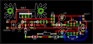
Like this ?
Attachments
Hi,
just had a quick look at the layout.
The link between power ground and signal ground is missing a link (via) right next to C5. Remember blue is the copper layer on the component (top) side.
Why are there overlaps in a prototype layout that was made for being easy, like C4/D4, C5/R6? Also, why mount R1/R3 vertically and all the other resistors horizontally?
And why so many different parts cases and placement variants (like different lead lengths on resistors, solder pitch on capacitors)? Many capacitors have equal case size, why not use the same footprint and lead spacings?
Doesn't Q1 require (or could benefit from) cooling? As your layout is two-sided anyway (why, actually? 😉), why not place it on the other side of KK1?
All in all, I'd say this layout could benefit from compacting and rerouting. You could still do it single sided, even with Q1 on KK1. 🙂
Cheers,
Sebastian.
I'm sorry, I was called at the phone and hadn't the time to write that :
- the layout is for p2p wiring on protoboard, not pcb (no via needed thus);
- hence overlaps, different sizes of resistors and so on are "creative bending" of leads, not different parts;
- both red and blue are under the board. I used red so it's easier to see. Blue is for the sensitive sense network.
- Q1 dissipate about 0.4W in my application. A small piece of aluminium will fit and be sufficient to keep the bd139 happy.
- i try to make use of the "stripes" of the protoboard, so the layout is certainly sub-optimal as far as size is concerned.
I will see if I can fit q2 on the heatsink though, good idea 🙂
00940 said:
I tried but I didn't get anything that'd make sense. I increased the resolution of the simulator but here is all I get. The graph with the a voltage variation is the output of the lm317 vs output current. The graph with no voltage variation to speak of is the output of the pass transistor vs output current. As load, I used a ccs with a pulse voltage source.
OK, much better, but the current change is really a slope rather than a pulse. Almost anything slapped together can cope with that.
You should make the rise/fall times of the current waveform something like 10uS, and then see what happens.
Jan Didden
Hi,
First an apology. I have built it !! In a lot of respects it's good, very good. I was wrong when I said a voltage reg properly deployed would probably be better.
This is what happened. First I havn't an LM317 so I fed the pass transistor from a lab PSU. I kept Q2 R4 etc and used a 3 volt zener across base and emmiter with 180 ohm for R4. This gave 12 ma current. Everything else as per circuit with a 6.8 zener feeding the ref to pin 3 of the IC.
First observation, decoupling more critical than you would believe. Even though fed from a PSU if C6 was not near the pass transistor circuit would oscillate at 20 Mhz at between 1.5 and 5 volts pk/pk. Adding compensation cap to 5534 made no difference. Get the decoupling right and the performance was excellent. I used a HEXFET fed by a generator at 15 hz and this switched a 90 ohm across the supply. A 'scope on 1 mv/div showed no easily measurable artifacts caused by the fast switching of the load. It was excellent. I then swapped the 5534 for a TL081 and the performance was unchanged except that all the stability issues dissappeared. You could ommit decoupling altogether, it didn't affect it.
Out of curiosity I tried the switched load on a 7812 , 7815 and l130 reg. In all cases a large spike of up to 60 mv was generated on pin 3.
The only downside is a relatively high quiescent current and a slightly high drop out.
Well done, I learnt something today 🙂
Congratulations ! You're the first one to bring "real life" inputs into this thread. Thanks a lot. 🙂
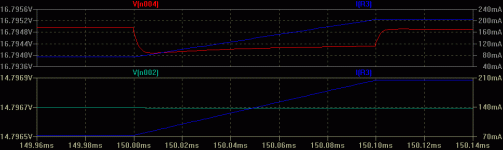
I'm surprised however when you say that the performance was unchanged when switching from the ne5534 to the tl081. I know that sims are never perfect but here are the results of a sudden change of voltage (0.1us rise time). With the ne5534, nothing moves, with the tl081, it's quite a big jump, similar to what you experienced with the three-pins regs.
I'm surprised however when you say that the performance was unchanged when switching from the ne5534 to the tl081. I know that sims are never perfect but here are the results of a sudden change of voltage (0.1us rise time). With the ne5534, nothing moves, with the tl081, it's quite a big jump, similar to what you experienced with the three-pins regs.
Attachments
Hi,
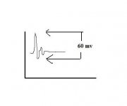
I nearly took some screen shots off the 'scope but there was nothing to see really. In contrast to the 7812 etc. I have drawn what that looked like showing over and undershoot as the output settles. The TLO81 is a bit weedy but it didn't affect things at all, just the reverse actually as far as stability goes. Might it be worth using a higher gain pass device and lowering the current source slightly and perhaps using a different opamp. The quiescent current on the TLO81 is much lower and the TLO61 is below 0.5 ma from memory. As I say though, the performance as a regulator was excellent, it really was, particularly under dynamic conditions. The generator I use has very fast rise times at these frequencies and this was coupled directly via a 2k7 resistor to the gate of the HEXFET and the drive offset to give a true 0 - 6 volt pulse on the gate.
So there you have it 🙂
Attachments
Well, I'll trust you and your scope on this, it's way better than put my trust into LTspice 😉
If one uses a bd139-16, a current source of 3ma is all that's needed for 300mA output (worst case).
If one uses a bd139-16, a current source of 3ma is all that's needed for 300mA output (worst case).
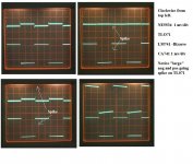
This is fun 🙂 Real pictures. Actually it's very interesting comparing Spice with reality. When I have time will post the shots of the 7812 for comparison. Remember this is just a breadboarded construction, not an optimised PCB.
The squarewave in all the shots is the signal on the drain of a HEXFET switching the load to ground. So "zero" or the lower part of the waveform is max current drawn by load. The amplitude of those spikes have to be taken in context, its very good really.
The squarewave in all the shots is the signal on the drain of a HEXFET switching the load to ground. So "zero" or the lower part of the waveform is max current drawn by load. The amplitude of those spikes have to be taken in context, its very good really.
Attachments
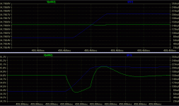
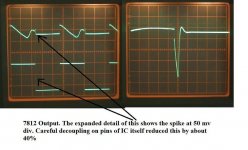
The 7812 with 90 ohm load as before. The settling time is poor. In order to get a stable photo I had to up the frequency of the switched load. It never recovers before the next pulse comes along. It was just over 100 hz here. I tried from around 10 hz up to several khz with the discrete version with little change. You need the higher speed to take pics unfortunately.
Attachments
Hi Andrew,
The 5534 does have a spike but it's small. I measured around 16 mv peak to peak, symetrical. ie 8 mv positive going 8 negative.
It wouldn't show in a picture clearly -- too much jitter for my camera.
What is interesting is the way parts from different manufacturers can give different results. That LM version of the 741 was weird.
Mooly said:The 7812 with 90 ohm load as before. The settling time is poor. In order to get a stable photo I had to up the frequency of the switched load. It never recovers before the next pulse comes along. It was just over 100 hz here. I tried from around 10 hz up to several khz with the discrete version with little change. You need the higher speed to take pics unfortunately.
Mooly, interesting pics!
What's the timebase here? It almost looks like a rectifier hum breakthrough at high loads.
Jan Didden
Hi Jan,
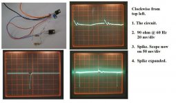
The 7812. A more careful implementation, the other was on a breadboard. The supply in the previous pics was a Farnell lab PSU feeding the 7812. Totally clean supply.
This is a 7812 fed from an unregulated 24 volt supply with a 6800 mfd reservoir cap. The reg has a Panasonic 220/35 v cap on pins 1 and 2 and a 47/16 volt cap on pins 2 and 3. It was soldered on the "rear" of the legs and is hidden in the picture. The FET switches 90 ohm ( 2 * 180 ) to ground. The scope was connected directly to the pins of the IC. The IC was an NEC7812. Temperature was just about acceptable freestanding, estimated at around 60 to 70 degrees C.
Attachments
- Status
- Not open for further replies.
- Home
- Amplifiers
- Power Supplies
- Low cost regulator in between Jung and Flea