MJL21193 said:...It's running very stable...
How stable is Iq with U4 not working (PNP with collector more positive than emitter) 😉
MJL21193 said:Nothing nasty when I remove power and it stabilizes quickly (no notable thump) on power up.
There is a slight hum but that is due to the makeshift power supply (just one 10mF cap). I expect that will subside when I do a proper supply with the higher voltage regulated front end supply.
It's running very stable, laying on the bench with wires dangling everywhere and no output inductor or Zobel.
Are you sure that R4/C2 filters the hum enough?
juma said:
How stable is Iq with U4 not working (PNP with collector more positive than emitter) 😉
Aha! You noticed...I made that mistake early on but left it in the schematic to see if anyone was actually paying attention.

Seriously. 🙂
It uses the 2SC3503 for Vbe and tracks fine. I'll post an up to date schematic just as soon as I get this computer straightened out (my screen capture utility - MS Paint is missing)
Wavebourn said:
Are you sure that R4/C2 filters the hum enough?
The schematic in post #1 does not have the bell and whistles: bypass, decoupling or RC filters and neither does the prototype - just the basics. The final design will have it all (eventually...time, never enough).
kipman725 said:I'm sure you could improve its performance by putting some nice global feedback in there.
Simulated THD is low and should give a good indication of the real thing (it has in the past with other amps).
Besides, add GFB and it becomes just another slightly different amp.
Member
Joined 2009
Paid Member
Am I understanding this amp ?
It is single ended at the front, but not at the output. It's Class A all the way through. With no global nfb the use of an LTP offers no benefit. The nice thing about dumping the LTP is that also gets away from dominant H3 that I see popping up in my sims.
But simple single ended front end usually aren't too linear. So you added a CCS to help out there. You added a common emitter amplifier to the input device to reduce the loading on it, thus providing a phase change and a simple chance to put some -ve feedback in place which does wonders for the linearity. The VAS is not bootstrapped, but linearized with a CCS too.
Why does Rick call it a differential transconductance - I can't see the "differential" part ?
Re: Oh!.... lovely scope!
Yes...but...what about the amp? 😉
To boring? To much the same?
I'm not sure I am myself! 😀
Good questions and observations Gareth.
Further playing around:
destroyer X said:
Oh!.... lovely scope!
Yes...but...what about the amp? 😉
To boring? To much the same?
Bigun said:Am I understanding this amp ?
I'm not sure I am myself! 😀
Good questions and observations Gareth.
Further playing around:
Attachments
MJL21193 said:
Besides, add GFB and it becomes just another slightly different amp.
Not necessary, if you add it, instead of replacing.
Hi John,
I'm confused by looking at your schematic. Do you use single or dual rail supply? C4 tells that you should use single rail supply, but then what is V1 for??
Nesa
I'm confused by looking at your schematic. Do you use single or dual rail supply? C4 tells that you should use single rail supply, but then what is V1 for??
Nesa
Member
Joined 2009
Paid Member
blueskynis said:, but then what is V1 for??
Once again, I'm blind. I left that in while I was trying different things. Corrected scheme below.
😱
Bigun said:So you couldn't resist the dual supply on the front end eh ? 🙂
I'm not as sharp as usual tonite - I'll get it all together...

Bigun,
Here's the story on the "differential transconductance amplifier". I'll try to explain, but think about it before you say I'm crazy.
In the discussion that follows, the voltages and currents I'm talking about are AC values. Assume the base of Q1 is the + input and the emitter is the - input of the amp. If the base to emitter voltage of Q1 increases (slightly), then the collector current of Q1 increases. This causes the currents through Q2 to increase. In turn, the voltage across R13 increases as does the voltage across R21. The (AC) currents through R13 and R21 are approximately the same, and the voltage at the emitter of Q1 is nearly the same as the voltage at the base. Note that this assumes a very high gain transistor, but it is a reasonable approximation for discussion purposes. Therefore, (Vc2-Ve1)/R13=Ve1/R21. After a little algebra, we get Vc2/Ve1=(R13+R21)/R21.
Rick
Is looking at it as the emitter of Q1 at the inverting input and the base as the non inverting clearer?
I made another update above. Changed the R4 pot value to 10K and R10=100K.
I made another update above. Changed the R4 pot value to 10K and R10=100K.
Member
Joined 2009
Paid Member
Rick,
Now I know what you mean. I had thought you meant something else, as you had said "In effect, Q1, Q2, Q3 and the associated components form a differential input transconductance amplifier" and I was off thinking that you thought Q3 was involved in a capacity other than a current source for Q1 and Q2.
I was thinking 'local negative feedback' and not 'differential' amplifier. I've been looking at LTPs for too long !!!
We're on the same page now.
Wavebourn said:
Not necessary, if you add it, instead of replacing.
I don't have anything against (global) feedback. I just wanted to do this amp without it. Seems to work well.
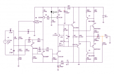
Final schematic for now - could be how I leave it:
I spent a bit of time playing with different output stage configurations without appreciable improvement. I think simple maybe best.
The next time you may want to try a source follower loaded on a counter-modulated CCS. However, it will require some servo.
That is a similar output stage used by Matti Otala in his groundbreaking design from years ago.
Jam
Jam
Member
Joined 2009
Paid Member
- Status
- Not open for further replies.
- Home
- Amplifiers
- Solid State
- Looking for Feedback on this No Feedback Amp.