Please don't take my comments in a wrong way. I am also interested in improving performance and going for best layout.
But I'm also very practical man and it's my experience, that sometimes things which might not seem "proper" from technical perspective, work very well in reality.
Not that I think anything is not proper on my recent layout. I actually want to use the board for common capacitor's grounds connection and for reference for OG taken form the same plane.
It simplifies matters when implementing different PS structures and sometimes people run those amps from batteries. As I mentioned earlier, SG is only for reference and it leaves all connection choices to you. But you need this reference pad on the board.
The layout is more compact than National's board, so any ground loops and other possible disturbances are greatly reduced.
As you all see, Kusunoki also doesn't use additional bypass caps. I never found them useful and when trying to install them directly at the big caps, I didn't like the sound of high frequencies.
PS: CF factor is quite important😉
Brian:
Ok... just for reference & confirmation.
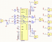
R1/R2: Feedback resistors
R3 = RI1 in National White Paper (National White Paper = NWP)
R4 = RIN in NWP
R5 = RI2 in NWP
R6/R7 = RB1 & RB2 in NWP
R8/R9 = ROUT1 & ROUT2 in NWP
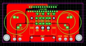
#1. Signal ground tied to power ground on board. SG is your star grounding point for all signal & tied via trace to power ground.
#2. Configured for Parallel operation. Stereo operation would require removing R8/R9 & lifting either R6 or R7 to split the input. Maybe another solder pad which would allow using this in stereo easily would be a good feature to add. R4 would also be removed for stereo.
Any corrections to this?
Ok... just for reference & confirmation.
R1/R2: Feedback resistors
R3 = RI1 in National White Paper (National White Paper = NWP)
R4 = RIN in NWP
R5 = RI2 in NWP
R6/R7 = RB1 & RB2 in NWP
R8/R9 = ROUT1 & ROUT2 in NWP
#1. Signal ground tied to power ground on board. SG is your star grounding point for all signal & tied via trace to power ground.
#2. Configured for Parallel operation. Stereo operation would require removing R8/R9 & lifting either R6 or R7 to split the input. Maybe another solder pad which would allow using this in stereo easily would be a good feature to add. R4 would also be removed for stereo.
Any corrections to this?
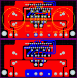
I was working today trying to simplify power planes and this is what I came with. I think I managed to preserved the "harmony" of the original 3870 board here😉
Continuous plane on V+ rail provides more current capability as well. I'm still not sure if V- plane has to be that large, but I want to keep it in a nice shape and cutting at 45 deg didn't look that well and additional elbow doesn't seem good either.
Continuous plane on V+ rail provides more current capability as well. I'm still not sure if V- plane has to be that large, but I want to keep it in a nice shape and cutting at 45 deg didn't look that well and additional elbow doesn't seem good either.
Attachments
Kevin Haskins said:Brian:
Ok... just for reference & confirmation.
R1/R2: Feedback resistors
R3 = RI1 in National White Paper (National White Paper = NWP)
R4 = RIN in NWP
R5 = RI2 in NWP
R6/R7 = RB1 & RB2 in NWP
R8/R9 = ROUT1 & ROUT2 in NWP
#1. Signal ground tied to power ground on board. SG is your star grounding point for all signal & tied via trace to power ground.
#2. Configured for Parallel operation. Stereo operation would require removing R8/R9 & lifting either R6 or R7 to split the input. Maybe another solder pad which would allow using this in stereo easily would be a good feature to add. R4 would also be removed for stereo.
Any corrections to this?
That looks correct. I attached a schematic to this document.
As for your questions:
#1. The signal gnd is tied to the power gnd through the trace going between the SG and IN pads.
#2. It is configured for parallel configuration. In order to do it for stereo operation, you would have to change the input and output pads, and add another 22k to GND for the other channel. This board is intended as a higher power solution, as the LM3875 board will cover the normal power version.
EDIT: As for the schematic below, I didn't specify the Mute resistor value, but it can be calculated from the datasheet as per the used power supply voltage.
--
Brian
Attachments

I would not recommend this board to run stereo amps. LM3875 sounds better in that aplication and provides more separation between channels, as two separate chips are used.
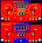
BrianGT said:I converted the pad to have heat relief traces on all of the pads connected to the planes, except for the LM4870 leads.
See the attached picture
--
Brian
Do you get that much expansion contraction?
Since you like to connect parts p2p, it could be easily done. Just don't solder one end of input and output resistors' leads (to the borad) and connect input wires and output wires directly to those leads. Also, shunting resistors can be mounted directly on RCA jacks😉
Kevin Haskins said:
Do you get that much expansion contraction?
Remember that the board is only 2.9" x 1.45" The heat relief traces will make soldering much easier.
The picture below seems to be the actual size on my screen.
--
Brian
Attachments
Peter's layout
I prefer Peter's layout at this stage. Very nice. Peter, could you post the bottom layer? Any chance you could make the link between SG and main gndplane optional meaning 1 extra pad for each????? pleeeeeese
Otherwise I'll be cutting it and jump-wiring.
-Robert
I prefer Peter's layout at this stage. Very nice. Peter, could you post the bottom layer? Any chance you could make the link between SG and main gndplane optional meaning 1 extra pad for each????? pleeeeeese
Otherwise I'll be cutting it and jump-wiring.
-Robert
Re: Peter's layout
It's no problem to make it. But how many people will really use that option? If only few, it would be probably easier for everybody to just cut the small trace😉
But I'll try to figure convenient way to keep everybody happy. One easy way to avoid using jumper would be placing pads (with shared hole) on both layers and soldering wire through them. But, then this prevents people from using resistor.
I still don't have bottom layer done. Will be working on it in the evening. I like those current plane arrangement, especially the ground plane, having more regular shape.
RFScheer said:Any chance you could make the link between SG and main gndplane optional meaning 1 extra pad for each????? pleeeeeese
It's no problem to make it. But how many people will really use that option? If only few, it would be probably easier for everybody to just cut the small trace😉
But I'll try to figure convenient way to keep everybody happy. One easy way to avoid using jumper would be placing pads (with shared hole) on both layers and soldering wire through them. But, then this prevents people from using resistor.
I still don't have bottom layer done. Will be working on it in the evening. I like those current plane arrangement, especially the ground plane, having more regular shape.
Now that you mention it...
Peter,
Agree 100% with you. If I'm the ONLY vote for a wacko ground connection, don't do it.
I was avoiding giving more advice, but now that you mention working on the bottom layer, there are some options for cutting the power and ground resistances in half and even achieving better separation of all the ground planes (only IF that is considered important though).
Anyway, it would be a shame to see much empty space on the bottom layer.
I had another idea but am pulling the zipper across my mouth before it's too late.
-Robert
p.s. - I am really having fun putting together 4 ch BrianGT NIGC amp atm. Am removing passive crossover from 2-way speakers and will drive from Linux PC using BruteFIR dsp crossover through 4 outputs of soundcard. This is all part of the PC music player thread over in Digital. Can't wait to hear it.
Re: Now that you mention it...
What exactly you have in mind? I could run some double planes on the bottom to increase conductivity, but other than that, I have no other ides to use that space.
I have to admit that ground and power planes are not something that I have much experience with. I mostly do it instinctively and to "look good"😉
RFScheer said:
I was avoiding giving more advice, but now that you mention working on the bottom layer, there are some options for cutting the power and ground resistances in half and even achieving better separation of all the ground planes (only IF that is considered important though).
What exactly you have in mind? I could run some double planes on the bottom to increase conductivity, but other than that, I have no other ides to use that space.
I have to admit that ground and power planes are not something that I have much experience with. I mostly do it instinctively and to "look good"😉
Nice!
Brian,
That's beautiful! Am I so tired that I'm hallucinating? Do I see isolated SG? I'll check back in the morning to make sure but it's great.
Wish I had time to check the trace to each pin of the ic, but I don't right now...
Peter is right that you should double up ground and power planes onto the bottom layer. Do this as much as possible and add a via near the inboard extreme edges. It's not revolutionary but WILL reduce resistance and especially will help ground noise (even though the middle section is constricted).
The idea I hesitated to mention was to solder on a surface mount wiring terminal strip (and simultaneous busbar) to the groundplane. You can eliminate some vias with this idea, improving groundplane layout and adding a huge shunt conductor in parallel. I really don't want to belabor this because we run the risk of spending lots of discussion and misunderstanding on rather small issues. Anyway, if you play with this idea, you will see that you can reduce the resistance of the groundplane an order of magnitude, without sacrificing looks or simplicity. As it stands now, the wiring pads cut into the width of groundplane substantially. But oops I'm getting far out on this limb, gotta stop before the branch breaks.
-Robert
I was planning continue with my layout today, but after seeing what Brian did here, there is no reason to look for anything else. This layout is very nice.
Looking further into it, it's actually beautiful and takes care of all previous issues. Good job, Brian😉
Looking further into it, it's actually beautiful and takes care of all previous issues. Good job, Brian😉
So nice!
Brian,
You are a true arteest.
Regarding the muting situation, you provided a spot for attaching a surface mount resistor between v- and pins 14 and 20 but there isn't a solder mask shape on the sm pads. Also, how would you actually use the mute? Don't you need an external pad to connect a toggle switch to?
-Robert
We usually treat mute as a resident evil. It is there, adjusted permanently, without any temptation on our side to use it in an actual amp😉
- Status
- Not open for further replies.
- Home
- Amplifiers
- Chip Amps
- LM4780 pcb layout and others