HF & MF Decoupling capacitors
1mF 25V electros are quite small, can often be made to fit the amp PCB and can be used for PSU up to +-22Vdc.
1mF 35V are a bit bigger and may fit, or change to 470uF 35V. These allow PSUs up to +-31Vdc to be used.
for the highest chipamp amp PSU voltages one must use 50V electros.
470uF 50V can usually be made to fit the smaller chipamp PCBs.
These allow any PSU upto the +-42Vdc limits of a 3886.
Those 470uF to 1mF cover the Medium Frequency (MF) Decoupling that should be fairly close to the chip power pins.
The High Frequency (HF) Decoupling often uses 100nF leaded X7R. These being small enough to fit on the power pins.
I have started using smd 220nF 50V and 1uF 50V in 805 package since I can get them even closer (less than 1mm) to the plastic package of the chipamp, rather than 3mm away from the plastic package.
XR7 resistors? You mean the X7R capacitors? Have another drink... 🙂
The 4.7 uF X7R modeled in TINA-TI was replaced with a 1 uF X7R in the actual circuit, as Mouser didn't have the 4.7 uF in stock. You should be able to recognize the 22 uF OSCON. The 1000 uF generic electrolytic can wasn't included in the LM3886 schematic. I assume that the reader has enough knowledge to read the LM3886 data sheet and include a sizable (470 uF or above) bypass cap at the power entry to the board.
~Tom

I'm knowledgeable enough to know, if this thing makes any type of sound at all, even transformer hum, it will be a success for me personally.
Actually if it does anything at all (i.e. make heat, light, smoke, open another dimension, etc.) that would be pretty positive.
I don't think that is enough.include a sizable (470 uF or above) bypass cap at the power entry to the board.
At the endge or entry to the PCB could be too far away from the chipamp power pins.
On the few PCBs that I have bought the MF decoupling is approximately 15mm to 20mm of trace length away from the power pins.
I would set myself a target of less than 15mm of trace length and as close to 10mm as I could achieve.
My HF decoupling has improved from ~3mm long leads to <1mm long leads into the package. That 1mm includes the power pin lead in the total lead length.
Those 470uF to 1mF cover the Medium Frequency (MF) Decoupling that should be fairly close to the chip power pins.
Depends on what you consider "medium frequency". The electrolytics cover the decoupling for most of the audio band.
The High Frequency (HF) Decoupling often uses 100nF leaded X7R. These being small enough to fit on the power pins.
I recognize that most people use 100 nF for the local decoupling. That actually doesn't do much. You can easily convince yourself of this by setting up a simulation and playing with the various capacitors. I did this and have documented the results on my Taming the LM3886 - Supply Decoupling page. Even with an optimistic estimate of the lead inductance of the LM3886, the supply impedance is still dominated by the lead inductance, not the impedance of the 100 nF capacitor. Hence, you want as much high-Q energy storage as close to the IC pin as you can get. This means the highest capacitance you can get rated for 50 V in X7R dielectric. That lands you around 1.0~4.7 uF.
I have started using smd 220nF 50V and 1uF 50V in 805 package since I can get them even closer (less than 1mm) to the plastic package of the chipamp, rather than 3mm away from the plastic package.
That's great, but it completely neglects the inductance of the lead frame, i.e. the part of the IC pin that's inside the package. You can have the IC X-rayed or dissolve the plastic to find out for sure, but I bet you're looking at at least a few mm of lead inside the package. That's another couple of nH of lead inductance. Then there's the bondwire itself. Even a double-bond adds 750 pH/mm and a triple-bond won't help much due to the mutual inductance between the bond wires. All in all, you're probably looking at at least 2~3 nH of inductance from where the pin enters the plastic package to the die itself. As you can calculate or see from my simulation, this means the supply impedance is dominated by the lead inductance at HF.
Decoupling at frequencies beyond 1 MHz (or perhaps a bit below) is supplied by on-die decoupling. You can't beat that.
My HF decoupling has improved from ~3mm long leads to <1mm long leads into the package. That 1mm includes the power pin lead in the total lead length.
That's great. What does the supply impedance look like after your modification?
My recommendation is to use the largest X7R cap you can get that can handle the rail voltage and put it as close to the IC as possible. Back that up with a 22 uF OSCON as close to the ceramic cap as possible. Use a 1000 uF cap at the power entry to the board (assuming the routing from the power entry to the LM3886 is reasonable). You can actually handle a bit of trace inductance on those nets and you can minimize the trace inductance by using pours or planes rather than traces for VCC, VEE, and GND.
I recommend the OSCONs for the intermediate cap as they tend to provide the lowest ESR and ESL of any of the electrolytic caps, hence, they will provide the lowest supply impedance.
I saw no benefit of increasing the power entry cap beyond 1000 uF in my simulation. At LF the supply impedance is dominated by the resistance of the wiring from the power entry caps to the rest of the power supply. Beyond 500 Hz, the on-board supply decoupling dominates the supply impedance.
~Tom
I recognize that most people use 100 nF for the local decoupling. That actually doesn't do much.
Yes, actually there is something that 100nF caps do very well, that's introducing a neat antiresonance peak in your Z that you can never get rid of, unless you add about 4-5 other caps with values spread between 100nF and the next larger cap.
As you say, it is much better to use the largest value you can get in 0805 size X7R/X5R dielectric . Much less problems...
Note that for example 6mm diameter 2.5mm pin spacing caps have about 4nH if mounted correctly, this means if you put 10 in parallel, you can have half the ESL of a ceramic, and many times more capacitance (but it is huge).
Yes, actually there is something that 100nF caps do very well, that's introducing a neat antiresonance peak in your Z that you can never get rid of, unless you add about 4-5 other caps with values spread between 100nF and the next larger cap.
Yep. I think the 100 nF "magic value" came about because for a long time it was the largest capacitance available in a low-cost ceramic dielectric. It certainly wasn't selected based on an analysis of the supply impedance.
As you say, it is much better to use the largest value you can get in 0805 size X7R/X5R dielectric . Much less problems...
Note that for example 6mm diameter 2.5mm pin spacing caps have about 4nH if mounted correctly, this means if you put 10 in parallel, you can have half the ESL of a ceramic, and many times more capacitance (but it is huge).
Even with SMD caps or many caps in parallel, the supply impedance will still be dominated by the several nH of lead inductance (including bondwire) of the LM3886. That said, a good SMD cap in 0805 or 0603 is probably as good as it gets.
One thing that many forget when they recommend multiple capacitors in parallel is the trace inductance between the capacitors. I experimented with that in my supply inductance simulation. I found that many leaded ceramic caps in parallel wouldn't actually help. You can do slightly better with SMD, but not much, actually... The best solution is still a large ceramic cap + 22 uF OSCON + 1000 uF electrolytic.
~Tom
One thing that many forget when they recommend multiple capacitors in parallel is the trace inductance between the capacitors. I experimented with that in my supply inductance simulation. I found that many leaded ceramic caps in parallel wouldn't actually help. You can do slightly better with SMD, but not much, actually... The best solution is still a large ceramic cap + 22 uF OSCON + 1000 uF electrolytic.
Paralleling low-ESR caps with traces = can of worms.
Leaded ceramics are useless, they have as much inductance as an electrolytic, so you may as well use one and get a lot more capacitance.
Standard 4 layer (0.2mm spacing between external copper pour and internal plane) gets you about 250pH/square which is nice.
Standard double-sided (1.55mm) is too thick, top/bottom planes are too far away, via inductance is huge, SMD ceramics can be used across a chip's pins but it's complicated.
I've done it Ghetto-style : take one piece of copper clad pcb, put all thru-hole caps on the edge, solder GND pins, apply kapton tape, then adhesive copper tape, then solder the other pins of caps to the copper tape. SMD ceramics on the edge of the copper tape. It is super effective because the kapton tape is thin (you can get like 100pH) but the copper tape is very thin and has high ESR (that can be useful for damping though). Even more ghetto is two thicker copper sheets with double sided adhesive between them, solder through-hole caps on the edge.
0.1mm double sided FR4 blanks or flex-pcb should work the same, but they're not commonly available.
tdk x7r 1 uf 100v smd is like 47 cents ea qty 10 at mouser, part number 810-FK16X7R2A105K
Last edited:
The important decoupling caps are not the ceramics but the ElectrolyticsThe best solution is still a large ceramic cap + 22 uF OSCON + 1000 uF electrolytic.
The have to be as close to the chip as physically possible and smaller values with smaller size is better than zillion uF if this means they are 1" further away.
The vital factor is the ESR. This is needed to damp the power rails AT the 3886. (In a discrete power amp, they need to be AT the output devices and also the VAS(s))
Good electrolytics have just about the correct amount of ESR to damp things properly. Bigger electrolytics need less ESR so this relationship is very serendipitious. But even 100u is good.
You can sim this in SPICE (just put in the inductance for your PSU tracks) for any discrete amp and also check this out in 'real life'.
The only caveat is that your electrolytics are very close to hot bits so will be the first thing to go after 15 yrs (for a good design).
The important effect is on stability with an extra bonus of better HF THD. They have to decouple to a 'dirty' earth so they don't muck up your 'clean' earths.
If you have the correct electrolytics in the correct place, extra ceramics bla bla don't make things worse but don't make things better either. 😱
Today, SMD ceramics might be more space efficient than electrolytics but you MUST have some series resistance, eg 0R1.
You can sim this in SPICE (just put in the inductance for your PSU tracks) for any discrete amp and also check this out in 'real life'.
That is exactly what I did. That's how I arrived at my recommendation of a 1.0~4.7 uF X7R ceramic cap (or larger if you can find it) right at the IC pins with a 22 uF OSCON as close to the ceramic as possible and a generic electrolytic can 470 uF or larger (I use 1000 uF) as close to the rest of the decoupling network as possible. In my Modulus-86, the power inlet connector is right up against the two 1000 uF capacitors.
You can see the simulation schematic and result on my website: Taming the LM3886 - Supply Decoupling.
In additional to the physical placement, it is important to minimize the trace inductance. I.e. use pours and planes rather than traces. Also, don't forget to minimize the inductance of the ground side of the decoupling network. Many designers get so focused on the VCC and VEE nets that they dork up the GND. This is true even when using a solid ground plane.
~Tom
This is precisely where the majority of Members get their layouts completely wrong.In additional to the physical placement, it is important to minimize the trace inductance..................... don't forget to minimize the inductance of the ground side of the decoupling network. Many designers get so focused on the VCC and VEE nets that they dork up the GND. This is true even when using a solid ground plane.
The Layout is the Circuit
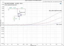
In case you are wondering about the impact of lead inductance in the feedback network, attached are some measurements.
The bottom trace shows the THD+N vs Frequency of my Modulus-86 R2.0 amplifier.
The middle trace shows the impact of the lead inductance of a capacitor in series with the feedback resistor to ground. The capacitor was mounted to the PCB Macgyver style with rather long leads.
The top trace shows the impact of 60 mm (~2.25") of AWG20 wire in series with the feedback resistor to ground. 60 mm of wire has an inductance of approx. 60 nH.
The measurement was done at 35 W output power into 8 Ω using 60 kHz measurement bandwidth on my Audio Precision APx525.
It is very clear that in a precision circuit, the layout matters. Even 60 nH is enough to degrade the THD by 10 dB at 20 kHz.
Tom
Attachments
The mantra should always be "minimum loop area" for feedback and other critical connections (clocks).
🙂
🙂
35 years ago, I used to use 100nF ceramic plus 22uF tantalum. This was purely down to size and price, 100nF Z5u would fit in a 0.1" pitch. I used to get resonance problems with video amplifiers, we were not really aware of the voltage dependence back then. These days I would use 1uF X5R in 0603 package
The mantra should always be "minimum loop area" for feedback and other critical connections (clocks).
🙂
The loop area was actually quite small as the wire was folded up. It's purely the lead inductance at play here.
I do agree on minimizing the loop areas as well, though. Loop area -> inductance.
Tom
Last edited:
And the closer you place and route critical components such as feedback components the smaller the loop, the less distance the traces need to go hence the reduction in parasitic lead inductance... Generally any analogue feedback be it op-amp circuitry or power supply feedback from a potential divider is best done with the minimum trace length possible from the pertinent pin, for op-amps as you have illustrated above, for power supplies because the FB inputs are quite often high impedance and thus very sensitive to noise etc....
That's... not how physics works. Inductance obtains solely from a loop integral in Maxell's equations so a structure cannot have inductance intrinsic to itself---its partial contribution to the total loop inductance always depends on the field distribution created in conjunction with the rest of the circuit. In conventional circuits it's common to ignore this consideration when working with such partial inductances, thereby making an assumption the field of the embodiment is a good approximation of whatever standard structure the reference partial inductance was calculated or measured in. In this case the structure sounds typical of a common DIYer hack but I'm not aware of any partial inductance reference values for lead inductance within it.The loop area was actually quite small as the wire was folded up. It's purely the lead inductance at play here.
Was this verified by measurement? The 1nH/mm rule of thumb for bond wires may be high by a factor of two or more depending on the geometry obtained by lead folding. 60mm sounds long for cap leads; if that's two leads of 30mm there may be another factor of two in play.60 mm of wire has a [partial] inductance of approx. 60 nH
Rather in depth discussion:
Assuming the folded lead geometry is consistent along its length you could work out the nH/mm by measuring at a few different points if you wanted to; measuring right where the leads exit the cap body would give reasonable ability to control for the partial inductance (ESL) of the cap proper. Note also inductance is a frequency dependent quantity with most structures transitioning between two asymptotic values at low and high frequency due to the shift from volume to surface conduction (so, typically, the lower asymptote is at more nH than the higher). Probably this isn't a big effect in this case but, if a ~GHz bond wire rule of thumb is being applied to ~20kHz here, it is an additional caution.
It's not really my intent to rain on the parade (even though I'm doing so 😉) but, in interests of offering suggestions towards greater clarity and robustness in the spirit of scientific peer review, I feel I should also point out the attribution is uncontrolled. Unbalancing ESLs by adding to R1 here reduces high frequency signal gain by -85dB from DC to 20kHz (-73dB DC to 80kHz), which has negligible effect on the 3886's local loop gain but might plausibly be expected to slightly increase the 3886's local THD as its ability to sense---and therefore correct---its harmonics is reduced as the gain rolled off. If this is the case, such errors should be attenuated by the control loop gain applied from the LME49710 in the Modulus-86. However, a quick look at these maths doesn't yield results in agreement with measurement, suggesting there may be other factors involved beyond uncertainty in the injected inductance. As the geometry's insufficiently described it's also unclear if the top and middle traces offer evidence to support or contradict.
One control I'd suggest, if there's interest in pursuing this, is measuring standalone 3886 behaviour to more accurately determine the amount and type of error being injected (an 19k:20k IMD FFT, for example, might offer helpful insight). Another is the hypothesis here predicts error should decrease as ESL is reduced or as feedback resistor values are increased. So one way round ESL uncertainties is to, say, double the 3886's local resistors, and see how much THD/IMD moves.
The 1nH/mm rule of thumb for bond wires
I measured AWG20 wire in college and found the 1 nH/mm rule of thumb to be a good estimate. The measurement was performed from 100 Hz to 40 MHz, as I recall, using an HP 4194A gain-phase/impedance analyzer. The inductance was extracted from the measurement using the equivalent circuits function on the instrument.
60mm sounds long for cap leads; if that's two leads of 30mm there may be another factor of two in play.
I didn't say anything about the lead length of the caps in my post from last night.
I just measured: ~50 mm lead length total. The cap was a Nichicon Muze bipolar. 1000 uF, 6.3 V.
I find it doubtful that the addition of a few 10s of mΩ to R1 will cause the rise in THD. That sounds like hand-waiving to me.
Tom
Last edited:
Hi Tomchr, thanks for posting your measurements. I had talked myself into believing that a small amount of inductance in the lower part of the feedback loop was a good thing. My reasoning was that it would reduce the gain at HF (in the same way that Ci reduces the gain at DC) and that this would increase stability.
- Home
- Amplifiers
- Chip Amps
- LM3886 PCB vs Point-to-Point (with data)