
Cool! 😎
Now on to some details:
#
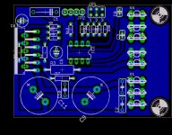
The feedback resistor R2 doesn't need to be any bigger than the rest, but it should have a direct, short connection to the chip. Try to give it it's own traces to pins 3 and 9 (independent to R7/R3).
#
The amp has to move left, you have to be able to mount it to a heatsink. Give it at least 1mm overlap over the board edge. Take care of R5, though. 😉
#
The ground copper does reach some of the parts only insufficiently. But sill, the grounding scheme of amp power ground, buffer power ground and signal ground looks difficult.
Normally, you would model this by giving the three grounds three different ground symbol designators from the libraries 'supply1' or 'supply2'. You don't have to. But keep in mind that the currents flowing between power and ground will influence noise and distortion quality of the finished amp. They must not overlap when flowing through the copper!
Look at C6, it only has this tiny little strip above C1 for it's currents to flow to amp power ground. Either try moving C1 a little lower or (better 🙂) move the copper trace between C1 and R9 up, so that the ground plane is cut underneath C1 and spreads from R9 to C6.
Look at R13, it connects to the same ground as C5 and C6. But it belongs to the buffer, so it refers to the buffer supply ground. Try rotating it 90degree and have it jump over the trace to R6. It then connects to the ground copper at JP1, which is derectly connected to the buffer supply ground. 😉
Look at JP1, it is only connected to it's ground by the little strip above the fast-on connector. Move the upper five ST6,3's down one grid step, that should be okay.
#
The buffer IC2 still has it's second amp IC2B open loop. It's better practice to mute it as Jürgen suggested. It's just one net/copper trace. Try invoking the second amp from IC2 and place it anywhere on the schematic, then give it a net between out and (-) in, then place a ground at it's (+) in. The trace fit's underneath the package of IC2, ground is already there. 🙂
Also I again recommend to buy C3/C8 in the same size as C2/C4/C10. Easier to buy less types of components and looks better. 😉
Note that if you plan to use anything better than the TL072, you'll have to integrate more parts near it to compensate and decouple.
#
Make the amp power supply and amp output tracks much wider. The ground copper under C7/C21 can be reduced to the same width as the supply tracks. Output can be of same width as amp power. Generally choose as much width as possible, you have plenty of room.
#
I would compact everything to the left, you can then reduce your board size to your original idea (or even smaller). In general, suplly traces should be as short as possible, ground copper should be of same width as supply copper, tracks with high current should be distant to tracks with sensitive signals and hot parts (such as power resistors) should not be close to sensitive parts (such as signal resistors and opamps). 😉
Cheers.
Now on to some details:
#
The feedback resistor R2 doesn't need to be any bigger than the rest, but it should have a direct, short connection to the chip. Try to give it it's own traces to pins 3 and 9 (independent to R7/R3).
#
The amp has to move left, you have to be able to mount it to a heatsink. Give it at least 1mm overlap over the board edge. Take care of R5, though. 😉
#
The ground copper does reach some of the parts only insufficiently. But sill, the grounding scheme of amp power ground, buffer power ground and signal ground looks difficult.
Normally, you would model this by giving the three grounds three different ground symbol designators from the libraries 'supply1' or 'supply2'. You don't have to. But keep in mind that the currents flowing between power and ground will influence noise and distortion quality of the finished amp. They must not overlap when flowing through the copper!
Look at C6, it only has this tiny little strip above C1 for it's currents to flow to amp power ground. Either try moving C1 a little lower or (better 🙂) move the copper trace between C1 and R9 up, so that the ground plane is cut underneath C1 and spreads from R9 to C6.
Look at R13, it connects to the same ground as C5 and C6. But it belongs to the buffer, so it refers to the buffer supply ground. Try rotating it 90degree and have it jump over the trace to R6. It then connects to the ground copper at JP1, which is derectly connected to the buffer supply ground. 😉
Look at JP1, it is only connected to it's ground by the little strip above the fast-on connector. Move the upper five ST6,3's down one grid step, that should be okay.
#
The buffer IC2 still has it's second amp IC2B open loop. It's better practice to mute it as Jürgen suggested. It's just one net/copper trace. Try invoking the second amp from IC2 and place it anywhere on the schematic, then give it a net between out and (-) in, then place a ground at it's (+) in. The trace fit's underneath the package of IC2, ground is already there. 🙂
Also I again recommend to buy C3/C8 in the same size as C2/C4/C10. Easier to buy less types of components and looks better. 😉
Note that if you plan to use anything better than the TL072, you'll have to integrate more parts near it to compensate and decouple.
#
Make the amp power supply and amp output tracks much wider. The ground copper under C7/C21 can be reduced to the same width as the supply tracks. Output can be of same width as amp power. Generally choose as much width as possible, you have plenty of room.
#
I would compact everything to the left, you can then reduce your board size to your original idea (or even smaller). In general, suplly traces should be as short as possible, ground copper should be of same width as supply copper, tracks with high current should be distant to tracks with sensitive signals and hot parts (such as power resistors) should not be close to sensitive parts (such as signal resistors and opamps). 😉
Cheers.
Hi again,
I received the project via email (upon request) and will fiddle around with it as soon as I find the time. 😎
But one thing is important: What do you want to use as a power supply?
I'm asking because nothing has been said about the PSUs so far.
The project requires an amp supply of +-20 to +-30V with a 60VA to 150VA trafo and a buffer supply of +-15V with about 5VA to 10VA, depending on what you want to connect and how much power you need.
It's also importand how you want to integrate the PSU with the amp(s) into an enclosure. If you're unsure, please do a search on the forum for gainclone or lm3886 supply or PSU and report back on what you decide to do.
Cheers,
Sebastian.
Move those dcoupling pins closer to their respective power pins... they are almost useless way out there...
You also need rectifiers and voltage regulators for the buffer (it can't use the same supply as the amp).
You can use the same trafo for amplifier and buffer, but not the same PSU output.
Project 115 from ESP contains a suggested PSU. Do you intend to use this?
You can use the same trafo for amplifier and buffer, but not the same PSU output.
Project 115 from ESP contains a suggested PSU. Do you intend to use this?
The Project 115 PSU already contains a supply connection (+-15V) for the buffer, so you don't absolutely need Project 05 additionally.
OTOH, P05 is of higher quality, but it won't fit on the board and will increase your PCB and parts costs.
OTOH, P05 is of higher quality, but it won't fit on the board and will increase your PCB and parts costs.
Hi,
okay, I know there are enough GC projects out there, but this one is special.
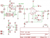
I have adapted and corrected the schematic. Now I want to know if I did it right. 😉
Please have a look and tell me what can be improved upon.
Constraints:
- schematic initially according to ESP projects 88 (buffer) and 19 (amp),
- split buffer and amplifier supplies,
- low component count due to small board size,
Changes to the former version:
- put documentation field on page,
- changed hole size from 2.8mm to 3.2mm (M3/3mm bolt plus washer diameter),
- replaced TL072 with TL071 (higher quality amps available in this package),
- separated PSU wirings from signal nets; split signal and power ground,
- adapted connector symbols in schematic to ease drawing,
- introduced star ground network with jumper (for optional resistor),
Okay, here goes.
Thanks,
Sebastian.
PS: The board is nearly finished, I just need corrections and critique. 🙂
okay, I know there are enough GC projects out there, but this one is special.
I have adapted and corrected the schematic. Now I want to know if I did it right. 😉
Please have a look and tell me what can be improved upon.
Constraints:
- schematic initially according to ESP projects 88 (buffer) and 19 (amp),
- split buffer and amplifier supplies,
- low component count due to small board size,
Changes to the former version:
- put documentation field on page,
- changed hole size from 2.8mm to 3.2mm (M3/3mm bolt plus washer diameter),
- replaced TL072 with TL071 (higher quality amps available in this package),
- separated PSU wirings from signal nets; split signal and power ground,
- adapted connector symbols in schematic to ease drawing,
- introduced star ground network with jumper (for optional resistor),
Okay, here goes.
Thanks,
Sebastian.
PS: The board is nearly finished, I just need corrections and critique. 🙂
Attachments
if the circuit is still open for debate... 😕
I won´t do it that way.
routing the naked in+ pin of the opamp to the input connectors is not a good thing. At least there should be a current limiting resistor. Maybe a resistor of reasonnable size is to small to offer good protection, but it gives a better feeling. 😉
This could also be used for impedance matching at jfet-inputs. Jfet opamps are supposed to be sensible to commonmode distortion.
I feel the dc-blocking capacitor is also best at the circuit input and not somewhere in the middle.
Regards
Jürgen
I wouldn't do it that way, too. 😉
But it's ESP Projects 19 and 88...
The cap in the middle is there in order to protect the potentiometer contact from corrosion due to DC bias currents.
An alternative option (that was already mentioned above) is to move the pot to the input.
But it's ESP Projects 19 and 88...
The cap in the middle is there in order to protect the potentiometer contact from corrosion due to DC bias currents.
An alternative option (that was already mentioned above) is to move the pot to the input.
ok, it´s reasonnable to stick with a real world design.
Maybe I was confused by your last schematic.
Regards
Jürgen
Maybe I was confused by your last schematic.
Regards
Jürgen
I recently found the time to determine component sizes, parts orientation and signal routing on the board. It came out as 40x45mm small, with the mounting holes and connector description print occupying the 'outer' 5mm. 😎
Roly, I now need to know what parts are available to you. After all, you (or anyone) should be able to build it... 😉
The following standard parts are to be on the current board:
- low power resistor packages '0204'
- 100nF cap sizes 2.5x5mm, pitch 2.5mm
- C1 value anything between 1uF and 4.7uF, size 7.5x7.5mm, pitch 5mm
- 200uF caps 35V, 8mm diameter, pitch 3.5mm
- 22uF caps 35V, 5mm diameter, pitch 2mm
- output resistor packages '0207' and '0411'
- buffer opamp like TL071, NE5534, OPA134 or OPA627 in package 'DIL8'
Please check your ability to source such parts in case you haven't got them. I need to know what parts you can get, so that the board has enough mounting space for the parts you (or everyone) wants to buy.
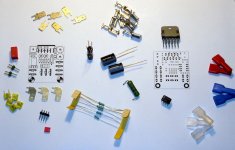
I took a picture of a layout print (in actual size) together with most components of the right size. See attachment. 🙂
Cheers,
Sebastian.
Roly, I now need to know what parts are available to you. After all, you (or anyone) should be able to build it... 😉
The following standard parts are to be on the current board:
- low power resistor packages '0204'
- 100nF cap sizes 2.5x5mm, pitch 2.5mm
- C1 value anything between 1uF and 4.7uF, size 7.5x7.5mm, pitch 5mm
- 200uF caps 35V, 8mm diameter, pitch 3.5mm
- 22uF caps 35V, 5mm diameter, pitch 2mm
- output resistor packages '0207' and '0411'
- buffer opamp like TL071, NE5534, OPA134 or OPA627 in package 'DIL8'
Please check your ability to source such parts in case you haven't got them. I need to know what parts you can get, so that the board has enough mounting space for the parts you (or everyone) wants to buy.
I took a picture of a layout print (in actual size) together with most components of the right size. See attachment. 🙂
Cheers,
Sebastian.
Attachments
Hi Roly,
hmmm. Good.
I will need a couple of days to resume on the layout, because I'm into work right now.
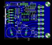
I attach the current state of development. Parts positioning is done but copper has still to be drawn, 'cause I've been waiting for the reply regarding the components choice.
The autorouter already proves that it fits on a single sided board, but it can use some readjustment and fine tuned layout by hand, which I currently don't have the time for.
Cheers,
Sebastian.
hmmm. Good.
I will need a couple of days to resume on the layout, because I'm into work right now.
I attach the current state of development. Parts positioning is done but copper has still to be drawn, 'cause I've been waiting for the reply regarding the components choice.
The autorouter already proves that it fits on a single sided board, but it can use some readjustment and fine tuned layout by hand, which I currently don't have the time for.
Cheers,
Sebastian.
Attachments
- Status
- Not open for further replies.
- Home
- Amplifiers
- Chip Amps
- LM3886 - P19, Any comment?