R5 value is wrong.
The minimum gain of the 3886 is 10times (+20dB).
The preferred gain used by many is 20times to 33times (+26 to +30dB).
With R6=22k & R5=82k the gain is set to 1+22/82 ~ 1.3times. You cannot go there.
You either have to increase R6 or decrease R5 or do a bit of both to get the gain into the range where the 3886 will be stable.
If you want to see an example of an amp that uses a film cap in the NFB loop look for JLH 80W FET amp. It uses very high values NFB resistors and a pair of 4u7F film in parallel to give some bass response.
Perhaps R5 was supposed to be 820R? This would give 28.9dB gain. If so, then C7 is sized a bit small to get decent bass. The resistor for the +ve input (here R3, 33k) needs to be the same value as the feedback resistor (R6, 22k) to get the lowest output offset.
if R5 were changed to 820r then C7 becomes greater than 3u3 * 33k * sqrt(2) / 0k82 >=188uF, use 220uF
Ah, I see. Thanks very much, Andrew (and abraxalito).
So...
Where R[in] = R3, R[nfb] = R6, R[nfb2] = R5, C[in] C6, C[nfb] = C7.
Gain = R[nfb] / R[nfb2] >10 <30 (20 seems a good target)
C[in](mF).R[in](ohms) =~90(ms)
C[nfb].R[nfb2]=~150
R[in] = R[nfb]
Hmmm... Will try some numbers.
So...
Where R[in] = R3, R[nfb] = R6, R[nfb2] = R5, C[in] C6, C[nfb] = C7.
Gain = R[nfb] / R[nfb2] >10 <30 (20 seems a good target)
C[in](mF).R[in](ohms) =~90(ms)
C[nfb].R[nfb2]=~150
R[in] = R[nfb]
Hmmm... Will try some numbers.
Last edited:
Put together simple excel spreadsheet.
2 examples shown.
1. Original idea with electrolytic NFB RC capacitor (but with resistor values corrected)
2. Film cap version requires some pretty extreme values to allow the NFB high pass capacitor to be film. 10uF is the largest film capacitor I have.
Will there be a possible noise problem with a 160k feedback resistor?
Attachments
Sorry for multiple posts.
Will stick with electro on the NFB loop. Get the thing built and the amp made. Once a test rig is up and running, I can try bypassing the elecrolytic and seeing if typical use shows any significant DC.
Will stick with electro on the NFB loop. Get the thing built and the amp made. Once a test rig is up and running, I can try bypassing the elecrolytic and seeing if typical use shows any significant DC.
Hi,
you have it.
Experiment with RC values to give the bass extension and bass strength that you need to sound right.
Amps that feed speakers without a bass driver can use much smaller RC values. This allows all film in the amplifier and much smaller PSU smoothing values.
A.) Gain = {R[nfb] / R[nfb2]} + 1 , for a non inverting amplifier block.
B.) Gain = Rupper/Rlower , for an inverting amplifier block.
Going back to A. if you insert a DC blocking capacitor that does not pass leakage current then the Rlower changes from R[nfb2] to R+C and at DC this is effectively infinity.
Any number divided by infinity equals zero.
Add 1 and you get the DC gain=1, when the DC blocking is perfect.
Last edited:
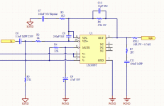
Yes. The past few posts hopefully dealt with that as I discovered the wonderful world of negative feedback. Unless my calculations are entirely wrong (that's quite possible) the new values discussed above for the feedback resistor, feedback high pass and input high pass components will provide workable gain and bandwidth. Schematic showing those components in place attached.The LM3886 is hard to get stable below gains of 10. Your gain setting is ~1,27.
Attachments
Hi,
this should work.
Decoupling must be close to the power pins and must connect to each other with very short tracks.
As an experiment, add a 1M0 pot across the 27k Rin.
Adjust the pot to bring the output offset to zero when warmed up.
Now switch off and let it all cool down. Switch on and monitor the output offset as the chipamp warms up from cold to operating temperature.
If this looks good then measure the pot setting and replace it with a fixed resistor.
This will change Rin slightly, maybe in the range 25k to 26k3.
Will use 100nF polyester capacitors on the underside of the PCB soldered directly to chip pins (midway between 1 & 5 for +V).Hi,
this should work.
Decoupling must be close to the power pins and must connect to each other with very short tracks.
As an experiment, add a 1M0 pot across the 27k Rin.
Adjust the pot to bring the output offset to zero when warmed up.
Now switch off and let it all cool down. Switch on and monitor the output offset as the chipamp warms up from cold to operating temperature.
If this looks good then measure the pot setting and replace it with a fixed resistor.
This will change Rin slightly, maybe in the range 25k to 26k3.
OK, I'll do that. Thanks very much.
routes will be even shorter if soldered to the top side pins.Will use 100nF polyester capacitors on the underside of the PCB soldered directly to chip pins (midway between 1 & 5 for +V)
That's why some solder decoupling direct to an opamp's pins rather than to the underside of a DIP socket.
Decoupling is specifically intended to meet VHF current demand.
Any extra inductance in the route lowers the frequency at which the decoupling is effective.
If the decoupling can meet all the VHF current demand then the traces and PSU only ever have to meet LF & HF current demand (equals less modulation of the supply rails).
Last edited:
Solder on the capacitors before inserting the chip into the PCB? Easy.routes will be even shorter if soldered to the top side pins.
That's why some solder decoupling direct to an opamp's pins rather than to the underside of a DIP socket.
Decoupling is specifically intended to meet VHF current demand.
Any extra inductance in the route lowers the frequency at which the decoupling is effective.
If the decoupling can meet all the VHF current demand then the traces and PSU only ever have to meet LF & HF current demand (equals less modulation of the supply rails).
Cheers.
- Status
- Not open for further replies.
- Home
- Amplifiers
- Chip Amps
- LM3886 on 1sided PCB design