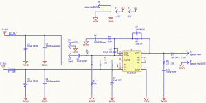
Oh, OK, the zobel network resistor just before output? Gotcha. It's 10R... Um, I'm looking at several example LM38xx designs and they're all 10R. I must have the wrong one.
I totally agree with you on the overall design philosophy even if I think the audio frequency spectrum several orders of magnitude too low for the boundary effect to be measurable.I have never talked to one, so I don't know. Although I wouldn't like changing direction, if I were one.
The more important reason is that electrons are reflected when they hit a border. The reflected ones superimpose on the ones that are still coming and the resulting wave is distorted. That is why HF cables are usually terminated with a resistor.
Would it be best to merge signal and power grounds on each chip's PCB?It has some drawbacks, too. You create long ground returns with (relatively) high inductance. The signal ground reference will have a slightly different potential than the power ground and ideally they should be the same.
:lol: I've not used an isolation transformer before and haven't had a need to look at one but rest assured I wouldn't just plug something into mains power without being sure I knew a great deal about it first!You see what I mean? You cannot use such a filter after an isolation transformer. The filter needs to be connected to PE. Nothing on the secondaries of an isolation transformer may be connected to PE, because that would defeat its purpose.
You may think it is safe. But you obviously do not yet have the technical background to make such an assessment.
Thanks for your comments! I'll have to change the amp-PCB layout to further minimise ground path length and look at linking power and signal ground.
Very probably. Generalising is always problematic. I was mainly motivated byYour layout apparently blindly follows the "Star Ground is best" philosophy. Star ground works well in some situations, but in others it's the antithesis of good design.
"When designing a layout, it is important to return the load
ground, the output compensation ground, and the low level
(feedback and input) grounds to the circuit board common
ground point through separate paths."
From the LM3886 datasheet design notes.
Obviously extrapolating that if separate signal paths are useful there, then they're useful everywhere is an unfortunate assumption.
Ah, I had wrongly assumed the distance to transformer ground was the important one but distance to the closest ground of the semiconductor being decoupled makes sense. I'll jiggle things around and see how it goes.This layout (in the first post) demonstrates the latter as far as your power supply bypass caps C6, C7, C10 and C9. They are indeed "physically near" the chipamp as they should be, but electrically (the important part) they're not. Each of their ground connections goes through a long trace to the "power ground" star ground, and the ground connection of the chip goes to the "Signal Ground" star ground. Presumably these two WILL be connected somewhere, preferrably (at least for this current layout) right there where they are. The circuit won't work without that connection. But the point related to these caps is they should have the shortest traces possible between their pins and the pins on the chipamp they connect to, otherwise they won't be doing their job. Each trace has resistance and inductance, and those increase with the length of the trace, and end up in series with these capacitors.
Thanks for the advice.Looking again at the layout, to get the shortest traces between them, these caps should be right beside the chipamp in the area now taken by R2, C1, R1, R4 and C2. The ground side of all four of these should connect together in one trace that goes to the ground pin of the chip.
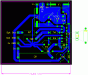
Usually 2mm pads. The screenshot isn't very useful in showing exact diameter and hole diameter.It looks like you are using very small pads. Unless you're having the board made professionally, I suggest increasing the pad diameter. I'd also advise against having floating planes of copper. Either scrap them or tie them to GND. I vote for scrapping them...
You'll need mounting holes...
~Tom
I'll remove the copper fill though I'm not sure what it could possibly do. Reflect RF radiation? I'd hope an audio circuit isn't generating any.
Good point with the mounting holes. 🙂
1mm of land around the hole gives plenty room to fit the soldering iron tip to for small and medium size component legs. Big heatsoaking legs can benefit from a bit more land.Usually 2mm pads.
Small legs can manage with 0.7mm of land. By the time land is down to 0.5mm things are getting quite small unless you are moving to SMT.
If you have a 0.5mm diam leg through a 0.7mm hole and use 0.7mm land the pad diameter would be 2.1mm. Your 2mm diam pad just about works for small components and small holes.
I'll widen things a bit for the larger components.1mm of land around the hole gives plenty room to fit the soldering iron tip to for small and medium size component legs. Big heatsoaking legs can benefit from a bit more land.
Small legs can manage with 0.7mm of land. By the time land is down to 0.5mm things are getting quite small unless you are moving to SMT.
If you have a 0.5mm diam leg through a 0.7mm hole and use 0.7mm land the pad diameter would be 2.1mm. Your 2mm diam pad just about works for small components and small holes.
---
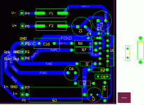
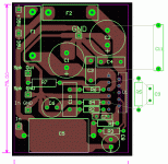
New PCB draft. Component positions and tracks not finalised - this is just to show amended ground path. Added speaker and input signal ground terminals. Feedback components will be mounted on the solder side.
Attachments
Last edited:
Advice from various people suggests signal ground should be linked to power ground within the chip-amp PCB area (which is what I tried to do there).C6 and R1 pass signal currents to the return routes.
These must connect to the signal ground.
Trying to implement
http://www.decdun.me.uk/gc/gcpsu.1t.2r.gif
"So the idea is that the returns to the power ground star are returned to the main ground star in the PSU without getting into the signal ground star. Still with me?
In theory, the wire going from the power ground star to the main ground star should be thicker than the wire connecting the signal ground star to it. Thicker wire, less resistance, so the 'pollution' flows to the main ground star and not into the signal ground star where it could affect the signal." [decibel dungeon]
Correction to my design: pin 7 is signal ground not power ground. ... Unfortunately this means advice to tightly connect V+/- supply pins to ground pin with decoupling caps is incorrect as they're separate ground networks. Back to previous design but less tortuous star routing on the power ground.
Last edited:
(damn this editing time limit!) I may well have misread advice on how to decouple the chip (very possible) but it does seem linking pin 7 to decoupling caps is incorrect.
Will have to make the link between signal and power ground thinner. Or add a resistor of a few ohms, though it's not a popular practice - seems to me like it would only be useful to compensate for a design flaw.
I've some OFC high amp automotive cable that should provide a low ipedence path to link PSU PCB and 2x amp PCB grounds. I've always wanted to use that stuff for something...
Looks like ground routing is fairly straightforward but I've been over-thinking it and making it more complicated than necessary.
Hi,
length of traces and/or cables probably gives more impedance than resistance.
If you compare the size of the output pin cross sectional area and length to your auto cable, you should realise that copper welding wire does not offer any improvement for domestic Audio.
length of traces and/or cables probably gives more impedance than resistance.
If you compare the size of the output pin cross sectional area and length to your auto cable, you should realise that copper welding wire does not offer any improvement for domestic Audio.
R7 in your first schematic. That belongs to the Zobel network parallel to the load. The datasheet recommends 2,7 Ohm and 0,25 W should be sufficient here. You use 3 times 8,2 Ohm 1 W in parallel, which is ~2,7 Ohm and 3 W.Oh, OK, the zobel network resistor just before output? Gotcha. It's 10R... Um, I'm looking at several example LM38xx designs and they're all 10R. I must have the wrong one.
Oh I see, sorry, I'm being dense. Yes, that makes sense. Thanks.R7 in your first schematic. That belongs to the Zobel network parallel to the load. The datasheet recommends 2,7 Ohm and 0,25 W should be sufficient here. You use 3 times 8,2 Ohm 1 W in parallel, which is ~2,7 Ohm and 3 W.
Hi,
length of traces and/or cables probably gives more impedance than resistance.
If you compare the size of the output pin cross sectional area and length to your auto cable, you should realise that copper welding wire does not offer any improvement for domestic Audio.
Interesting. Thanks.
Nice work
Hi
What a diffrence a lot of thought and direction make Nice work.
im not sure if it will make much diffrence but i suggest moving the audio in pad closer to input cap. Also i think a little more thought to getting the decoupling capacitors 0.1 uF closer to the chip it really is a worth while effort towards sound quality.I cheated i used double sided. Im no expert just a very happy newbie. And with a layout like that i know you will be very happy with your amplifier.
Regards ian
Thanks. I have to agree about the decoupling caps. I'll add them to the growing list of components to solder to bottom side. Will mean I can move the electrolytic capacitors a little closer too.Hi
What a diffrence a lot of thought and direction make Nice work.
im not sure if it will make much diffrence but i suggest moving the audio in pad closer to input cap. Also i think a little more thought to getting the decoupling capacitors 0.1 uF closer to the chip it really is a worth while effort towards sound quality.I cheated i used double sided. Im no expert just a very happy newbie. And with a layout like that i know you will be very happy with your amplifier.
Regards ian
Cheers...
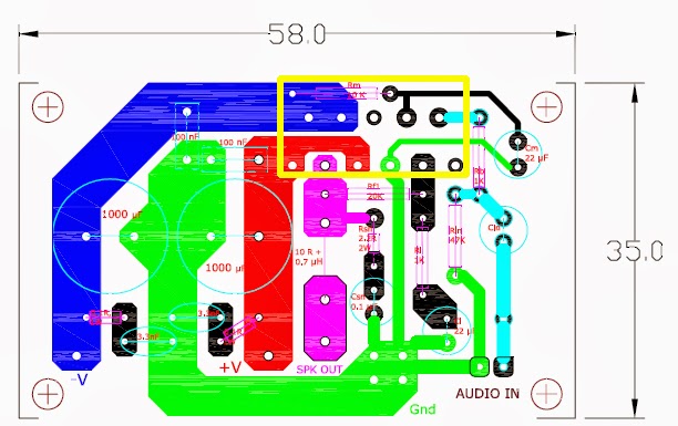
Latest and hopefully last design. Comments, suggestions, corrections welcome.
Components show as off the board are to be soldered to the underside.
your speaker ground Must not be connected with signal star ground. Speaker ground should connect straight to PS ground.
In fact you can tap the ground track going for C8 for spk gnd.
Last edited:
C9=100pF might be too big.
Expect a much lower value or even omit.
Connect C3 directly to C4 and tie that junction to the Power Ground.
Insert a location for a low value resistor between Signal Ground and Power Ground. You can use a resistor (1r0 to 100r) or a 0r0 link.
The Zobel and the Speaker returns must not connect to the Signal Ground.
Increase the land around pin4, remove pin2 if necessary (or include pin2 in the supply trace).
Last edited:
your speaker ground Must not be connected with signal star ground. Speaker ground should connect straight to PS ground.
I agree. You appear to have adopted a two-star grounding system. This might make some sense if all signal level signals (clean) met at one star and all the power (dirty) signals met at the other. But instead, you've introduced a high current carrying track between the two stars - that of the speaker return current. This will compromise your decoupling (as just one bad side-effect) as the speaker current wants to return to its source, the local decouplers.
- Status
- Not open for further replies.
- Home
- Amplifiers
- Chip Amps
- LM3886 on 1sided PCB design