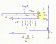
A fair amount of optional components here.
I may end up taking out the Zobel network as I doubt I'll be buying highly capacitive speaker wire and am driving efficient Warfdale 8 ohm bookshelf speakers.
While star earthing is unnecessary at this level, I thought, 'what the hell' and tried it anyway. It was certainly a challenge.
I could probably drop the 1uF decoupling MKT capacitors as they seem superfluous.
Comments, suggestions and corrections very welcome... 🙂
Attachments
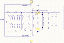
PSU design
Regulated power supply.
I'm dubious MKTs will be useful when the electrolytic capacitors are low ESR. I'm aware there's some controversy about bypassing bypass capacitors with smaller ones.
Regulated power supply.
I'm dubious MKTs will be useful when the electrolytic capacitors are low ESR. I'm aware there's some controversy about bypassing bypass capacitors with smaller ones.
Attachments
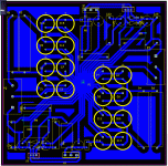
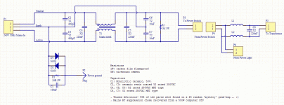
Mains RF EMI filter
Pre-transformer RFI filter stage for this amp. Standard sort of design. Safety link between Earth and power-ground copied shamelessly from Power Supply for Power Amplifiers
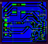
The PCB diagram looks a bit weird because at that point I hadn't worked out how to use Altium (trial edition) properly! 🙂
I've built this and run preliminary tests.
Pre-transformer RFI filter stage for this amp. Standard sort of design. Safety link between Earth and power-ground copied shamelessly from Power Supply for Power Amplifiers
The PCB diagram looks a bit weird because at that point I hadn't worked out how to use Altium (trial edition) properly! 🙂
I've built this and run preliminary tests.
Attachments
Last edited:
Hi
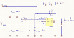
Im working on a lm3886 pcb at the moment . The biggest problem im finding is with the psu decoupling caps at the ic the ones you have marked C6 and C9. it is easy to get C6 close to the ic but i can find no way to get C9 closer. i had tried C9 in the same location as you a and after some reading find it is best to solder the cap directly to -v pin and using a cap with very small pin spacing 2.5mm would be good 5mm is easier and over 10mm could be problems when you add the length of the track into the equation it would lead to a high chance of being affected by inductance wich will render this decoupling cap as quite usless. Im quite new to this but im sure the imfomation i give is correct as it came from a very good source. Also it is a good idea to mount the feedback resistor to the ic as well to help keep the fb path ultra short. I wanted my pcb to contain all the parts in a nice neat way but if that will affect sound quality then it is a deff no for me. ps it is not over the top to use a star ground with this ic in fact id say it is law.
Best regards ian
I should point out the mains input is a 10A IEC connector with integrated fuse, the transformer is at the moment a 160VA 30+30V but once testing is complete I'll buy a 300VA model. The tranformer has two 4n7 capacitors wired across its secondaries as per http://www.diyaudio.com/forums/chip-amps/128278-tuning-ps-transformer-gainclone.html (replaced with 8n2 when I get the 300VA).
Yet to finalise a buffer PSU - this amp will include a discreet FET buffer from STEREO FET BUFFER FOR DAC, PREAMPLIFIER, TAPE REC, ... - eBay, Other, Computers Networking. (end time 06-Nov-10 03:41:04 AEDST) - with some component substitution, it's got some good reviews both on and off these forums.
Yet to finalise a buffer PSU - this amp will include a discreet FET buffer from STEREO FET BUFFER FOR DAC, PREAMPLIFIER, TAPE REC, ... - eBay, Other, Computers Networking. (end time 06-Nov-10 03:41:04 AEDST) - with some component substitution, it's got some good reviews both on and off these forums.
is pin 7 supposed to connect to power ground and not s ground and inputs and outputs should be kept as far away as possible from each other. maybe Andrew t would like to comment as it will give me a chance to see if im learning anything and to help us both build good sounding amplifiers.
best Regards Ian
best Regards Ian
Hi
Im working on a lm3886 pcb at the moment . The biggest problem im finding is with the psu decoupling caps at the ic the ones you have marked C6 and C9. it is easy to get C6 close to the ic but i can find no way to get C9 closer. i had tried C9 in the same location as you a and after some reading find it is best to solder the cap directly to -v pin and using a cap with very small pin spacing 2.5mm would be good 5mm is easier and over 10mm could be problems when you add the length of the track into the equation it would lead to a high chance of being affected by inductance wich will render this decoupling cap as quite usless. Im quite new to this but im sure the imfomation i give is correct as it came from a very good source. Also it is a good idea to mount the feedback resistor to the ic as well to help keep the fb path ultra short. I wanted my pcb to contain all the parts in a nice neat way but if that will affect sound quality then it is a deff no for me. ps it is not over the top to use a star ground with this ic in fact id say it is law.
Best regards ian
Thanks. Soldering components to the underside of the PCB is still neater than pin-to-pin construction and seems perfectly reasonable to me.
You need to use a star ground between amp units, power supply, input and output etc but many, many chip-amp PCB designs use what could be charitably called 'rail topology' without problem, though I still prefer star ground on principle.
Hi,
where did that 3886 schematic come from?
It is so difficult to read.
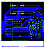
The PCB layout is unlike anything I have ever seen.
where did that 3886 schematic come from?
It is so difficult to read.
The PCB layout is unlike anything I have ever seen.
Hi,the transformer is at the moment a 160VA 30+30V but once testing is complete I'll buy a 300VA model.
if you get that far.
30+30Vac is very high and is very likely to take the supply pins well outside Nationals' recommended voltage range.
R1 does not need to be 5W and there is no advantage in using anything over 500mW.Pre-transformer RFI filter stage for this amp. Standard sort of design. Safety link between Earth and power-ground copied shamelessly from
The maximum voltage across the resistor will never exceed Vf of the diodes when passing Fault current.
Can your diodes pass Fault current until the fuse blows and the arc extinguishes?
Back to the resistor.
If Fault Vf=2Vpk the Pr~400mWpk for a few ms (or us).
Check the muting section. The capacitor should be between GND and pin 8.
The snubber resistor is oversized. A single 0,25 W resistor should do. If it doesn't hold, a bigger resistor will cure the symptoms, not the cause.
The high pass filter in the feedback loop has a higher roll-off than the input filter. It should be lower or equal.
Unused planes should either be grounded or deleted.
Traces with right angles should be avoided. Use curves or 45° angles.
Speaker traces should be far away from signal traces or components.
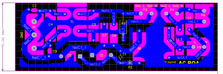
The regulated power supply PCB is really peculiar. It will be a great learning experience for you, if you try to realize it like that. Whether about mixing the positive input with the negative output on one connector or terminal and vice versa, whether about the way to mount a heatsink to the regulators and transistors, whether about using several star grounds (2 on the amp PCB, 1 on the power supply PCB), and so on.
And for safety's sake forget about building your own mains filter.
The snubber resistor is oversized. A single 0,25 W resistor should do. If it doesn't hold, a bigger resistor will cure the symptoms, not the cause.
The high pass filter in the feedback loop has a higher roll-off than the input filter. It should be lower or equal.
Unused planes should either be grounded or deleted.
Traces with right angles should be avoided. Use curves or 45° angles.
Speaker traces should be far away from signal traces or components.
The regulated power supply PCB is really peculiar. It will be a great learning experience for you, if you try to realize it like that. Whether about mixing the positive input with the negative output on one connector or terminal and vice versa, whether about the way to mount a heatsink to the regulators and transistors, whether about using several star grounds (2 on the amp PCB, 1 on the power supply PCB), and so on.
And for safety's sake forget about building your own mains filter.
Hi,
where did that 3886 schematic come from?
It is so difficult to read.
The PCB layout is unlike anything I have ever seen.
Me. It is horrible, I know. Will re-draft it.
With the software I'm using the components on the schematic need to match the components on the PCB: if I'm using a terminal block, the schematic also needs a terminal block and signal paths have to go to the block as well. This makes for a messy schematic.
I'll remove the 1uF bypass capacitors. That will free up room for wider, shorter track paths. Also swap output and signal ground terminals to move input and output away from each other and separated by ground tracks. I'm appliying star topology to the power ground, which hardly anyone else bothers with and I imagine that is why it looks a strange and overcrouded.
You're absolutely right. The mute delay capacitor and resistor must have got swapped around by accident at some point. Thanks!Check the muting section. The capacitor should be between GND and pin 8.
Which, where, when, who? Which resistor are you referring to?The snubber resistor is oversized. A single 0,25 W resistor should do. If it doesn't hold, a bigger resistor will cure the symptoms, not the cause.
1. I have yet to understand how impedence is calulated for different parts of the circuit in order to calculate roll-off frequency (the calculation is the easy part). I believe Andrew T said the opposite http://www.diyaudio.com/forums/chip-amps/174893-capacitor-question.html : The input filter should constrain frequency (have a higher HP roll-off) not the feedback filter.The high pass filter in the feedback loop has a higher roll-off than the input filter. It should be lower or equal.
Single copper plane. No additional layers to deal with (otherwise grounding would be much easier).Unused planes should either be grounded or deleted.
Because electrons hate having to change direction suddenly? 🙂 I'm simplifying the chip-amp PCB - fewer bypass capacitors will make room for better layout.Traces with right angles should be avoided. Use curves or 45° angles.
Good point. Already mentioned by AmpImp. Am fixing.Speaker traces should be far away from signal traces or components.
Thankyou, I aim to please! 🙂The regulated power supply PCB is really peculiar.
Yeah, it's a bit ugly. I'd better change it and have separate terminal blocks.It will be a great learning experience for you, if you try to realize it like that. Whether about mixing the positive input with the negative output on one connector or terminal and vice versa
Not a problem. This was designed around the heatsinks which are on either side of the PCB.whether about the way to mount a heatsink to the regulators and transistors
. I could use binding-posts/pins on the amp PCB to run all ground lines to the star via separate cables. Never seen it done but it's quite feasible and would simplify the amp PCB hugely. Mm, I like that idea.whether about using several star grounds (2 on the amp PCB, 1 on the power supply PCB)
Built it, tested it for obvious defects like shorts. I'll attach it to the mains via some current limitation for full testing (and it would be nice to get an isolation transformer sometime in the next few weeks). It's about as safe as anything connected to 240V can be. Will post photographs once tested fully.And for safety's sake forget about building your own mains filter.
Thanks for all suggestions and for pointing out the mistake with Mute. Cheers.
Last edited:
Improved amp PCB and schematics. Fixed issues with mute circuit, output being close to input. Changed from screw-down terminals to solderable binding posts to save room. Wider ground tracks. Removed 1uF decoupling capacitors. Cleaned up schematic. Adjusted C9 to more closely match an example circuit (Silicone Chip magazine's schematic).
Attachments
we are both agreeing the same design philosophy.
The input filter must set the bandwidth.
Look at your latest schematic.
Input filter 10uF & 22k gives F-3dB~0.7Hz, RC=220ms
NFB roll off 100uF & 1k gives F-3dB~1.6Hz, RC=100ms.
I recommend that the NFB RC>150ms and input filters of RC~90ms and 0.5us to 1us.
the mute still looks wrong.
If you can't read your own schematic then change your software.
we are both agreeing the same design philosophy.
The input filter must set the bandwidth.
Look at your latest schematic.
Input filter 10uF & 22k gives F-3dB~0.7Hz, RC=220ms
NFB roll off 100uF & 1k gives F-3dB~1.6Hz, RC=100ms.
I recommend that the NFB RC>150ms and input filters of RC~90ms and 0.5us to 1us.
the mute still looks wrong.
If you can't read your own schematic then change your software.
The mute is tragically, embarrassingly wrong. *sigh*
Changing Ri in the NFB to 1k5 gets 155ms.
For the input filter, 3.3uF and 2k7 should give about 89ms and the PCB will enjoy a much smaller input capacitor to boot.
I now understand RC filters and time constants. That helps a lot!
Thanks so much for your help here.
R7Which, where, when, who? Which resistor are you referring to?
I have never talked to one, so I don't know. Although I wouldn't like changing direction, if I were one.Because electrons hate having to change direction suddenly? 🙂
The more important reason is that electrons are reflected when they hit a border. The reflected ones superimpose on the ones that are still coming and the resulting wave is distorted. That is why HF cables are usually terminated with a resistor.
I could use binding-posts/pins on the amp PCB to run all ground lines to the star via separate cables. Never seen it done but it's quite feasible and would simplify the amp PCB hugely. Mm, I like that idea.
It has some drawbacks, too. You create long ground returns with (relatively) high inductance. The signal ground reference will have a slightly different potential than the power ground and ideally they should be the same.
Built it, tested it for obvious defects like shorts. I'll attach it to the mains via some current limitation for full testing (and it would be nice to get an isolation transformer sometime in the next few weeks). It's about as safe as anything connected to 240V can be.
You see what I mean? You cannot use such a filter after an isolation transformer. The filter needs to be connected to PE. Nothing on the secondaries of an isolation transformer may be connected to PE, because that would defeat its purpose.
You may think it is safe. But you obviously do not yet have the technical background to make such an assessment.
Your layout apparently blindly follows the "Star Ground is best" philosophy. Star ground works well in some situations, but in others it's the antithesis of good design.
This layout (in the first post) demonstrates the latter as far as your power supply bypass caps C6, C7, C10 and C9. They are indeed "physically near" the chipamp as they should be, but electrically (the important part) they're not. Each of their ground connections goes through a long trace to the "power ground" star ground, and the ground connection of the chip goes to the "Signal Ground" star ground. Presumably these two WILL be connected somewhere, preferrably (at least for this current layout) right there where they are. The circuit won't work without that connection. But the point related to these caps is they should have the shortest traces possible between their pins and the pins on the chipamp they connect to, otherwise they won't be doing their job. Each trace has resistance and inductance, and those increase with the length of the trace, and end up in series with these capacitors.
Looking again at the layout, to get the shortest traces between them, these caps should be right beside the chipamp in the area now taken by R2, C1, R1, R4 and C2. The ground side of all four of these should connect together in one trace that goes to the ground pin of the chip.
It looks like you are using very small pads. Unless you're having the board made professionally, I suggest increasing the pad diameter. I'd also advise against having floating planes of copper. Either scrap them or tie them to GND. I vote for scrapping them...
You'll need mounting holes...
~Tom
You'll need mounting holes...
~Tom
- Status
- Not open for further replies.
- Home
- Amplifiers
- Chip Amps
- LM3886 on 1sided PCB design