After building a set of LM3886 amps based on the Linkwitz circuit (which I really like!), I figured I would try an amp using the LM4780 based on the same circuit layout. Since I haven't used this chip before, I figured I would ask:
1) If anyone has used the Linkwitz circuit ( http://www.linkwitzlab.com/images/graphics/3886amp.gif ) using the LM4780 as two LM3886's. I know other amps (Brian and Peter's come to the front of my mind) use this chip in a similar manner, but I was specifically interested to see if anyone has used the Linkwitz topology. It should be fine, but there is no since in re-inventing the wheel if there is someone who has already found out any issues. (Searching the forum didn’t show much, but I figured someone has to have done this!!!)
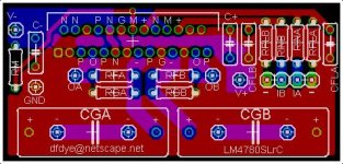
And 2) Attached is a proposed PCB that fell together rather nicely, but I figured I would run it past more experienced designers first. Particularly, I am concerned about the V+ section coming from the input pin header to C+ and the input signal traces running along the top right edge of the board. If anyone has any comments either way as to whether my concerns are justified, or if I am in good shape, I would appreciate the feedback. Any suggestions or comments about the rest of the board are welcomed as well!
Thanks!
David
As a side note, I started off trying to make this a single sided PCB. That idea got trashed rather quickly, but I was wondering if anyone has used a single sided LM4780 PCB?
1) If anyone has used the Linkwitz circuit ( http://www.linkwitzlab.com/images/graphics/3886amp.gif ) using the LM4780 as two LM3886's. I know other amps (Brian and Peter's come to the front of my mind) use this chip in a similar manner, but I was specifically interested to see if anyone has used the Linkwitz topology. It should be fine, but there is no since in re-inventing the wheel if there is someone who has already found out any issues. (Searching the forum didn’t show much, but I figured someone has to have done this!!!)
And 2) Attached is a proposed PCB that fell together rather nicely, but I figured I would run it past more experienced designers first. Particularly, I am concerned about the V+ section coming from the input pin header to C+ and the input signal traces running along the top right edge of the board. If anyone has any comments either way as to whether my concerns are justified, or if I am in good shape, I would appreciate the feedback. Any suggestions or comments about the rest of the board are welcomed as well!
Thanks!
David
As a side note, I started off trying to make this a single sided PCB. That idea got trashed rather quickly, but I was wondering if anyone has used a single sided LM4780 PCB?
Attachments
Well, I hope nobody finds anything! I just dropped in a prototype order (with a bunch of other stuff too . . . ) so I guess we will see how it comes out!
David
David
do you mean to use additional opamps, or use the LM4780 itself as one of the components in a filter network?
I am not sure I understand you question. I am using the LM4780 as the amplifier, not a filter.jackinnj said:do you mean to use additional opamps, or use the LM4780 itself as one of the components in a filter network?
(If I misunderstand your question, please forgive the basics. . . .)
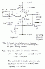
I am treating the LM4780 as two LM3886's. If any additional filtering is required, I will indeed use external components. I am currently planning on using these as part of a multichanel amp that will drive actively filtered speakers, so yes, I will be using additional opamps as a filter network, but I am not considering the LM3886's to be part of that filter network. The exception is if I use the two 220uf electrolytics in CGA/B instead of a 10uf film cap. This effectively filters most of the high end response if you are using these amps for woofers. This amp layout is pulled right from linkwitzlab.com, but I guess a copy of the schematic might be helpful. The Ci* cap does add a filtering, but again, that is not really the point of this circuit.
If this is not what you were asking, sorry for the tangent. 😀
David
Attachments
Thanks! I'll let you know when I get the amps built and tested.morgandc said:just letting you know that someone is reading your thread with interest...
-Dwight
David
Looks pretty good. I'm having a hard time keeping the output stable in a bridged configuration. Make sure you use small bypass caps very close to the chip and keep leads short and neat. Ballast resistors are required if you plan to bridge channels.
Rail lines are too slim, David. Image it in real size and imagine, that there should " flow " 10 A....
Using the overture series chips as part of an active filter has been tried -- not by me -- I haven't heard (or seen) any results published so I wonder if it is stable in this app.dfdye said:I am not sure I understand you question. I am using the LM4780 as the amplifier, not a filter.
Ah, now your question makes more sense. I am not sure, but I have not tried it in that configuration.jackinnj said:I haven't heard (or seen) any results published so I wonder if it is stable in this app.
David
dfdye said:... The exception is if I use the two 220uf electrolytics in CGA/B instead of a 10uf film cap. This effectively filters most of the high end response if you are using these amps for woofers.
How can you say that?
These caps form a hipass filter and do not filter the the high frequency response - no they tailor the lower frequency range for the midrange/tweeters if they have smaller values - it is all clear in the schematic drawing. The lopass filter - if you may call it like that - which tailors the high frequency response range is situated at the amps input.
Yea, I would generally agree with that. I was thinking I could get away with them because of the short runs, but I will definitely put a little more effort into beefing them up. The problem comes in with getting the power runs thick enough while getting them to all the Power pins. I really don't know enough about this chip to comfortably leave pins unconnected, but I agree getting full current to all pins should be a goal.Upupa Epops said:Rail lines are too slim, David. Image it in real size and imagine, that there should " flow " 10 A....
After reconsidering, I think there are better PCB layouts for this chip that would allow it some more breathing room (current that is.) The schematic from Linkwitz does seem solid though.
I find routing power in from the left side to be most effective with this chip. I have a small PCB I've done (1.5"x3") and that includes room to mess with some of Carlos's tweaks, bigger caps at the chip (2200 on mine), and paralleled output. Would be exceedingly simple to modify for two discrete channels. I'm still working on transferring it to Eagle. Prototype I have runs gret - stable, quiet...
C
C
Second! I would love to see other people's ideas about this too!alexcd said:CJD do you mind posting your PCB layout and schematic here?
David
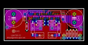
Along those lines, I also have a couple of board designs to take advantage of on board power regulation. I am not really happy with either of these yet, but I figured I would post them to let you guys have a look at my thinking. Keep in mind that they are still very rough drafts, but feel free to rip into them if you have suggestions!!!cjd said:I have a small PCB I've done (1.5"x3") and that includes room to mess with some of Carlos's tweaks, bigger caps at the chip (2200 on mine), and paralleled output.
I especially don't like having the input traces run past the V+ trace in rD, but if I put the input signals in front of the chip, I have to run them past a NC pin as in rE (also the traces are much messier in rE even thought the component layout is much cleaner). I am thinking about clipping the NC pins and running signals under the positions where those pads would go, but I haven't gone quite that far yet.
This is the rD board:
Attachments
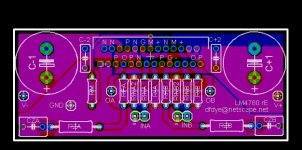
Rev E is a beautiful layout! Very symmetrical!
Sorry you had to go through several iterations, however you have come up with a winner!
Sorry you had to go through several iterations, however you have come up with a winner!
- Home
- Amplifiers
- Chip Amps
- Linkwitz LM4780 PCB Proposal: Comments Wanted!