marcus66 said:I'm sorry if my post above was against the rules! I did check the forum rules and moderator's statement, and assumed the subject to be OK, but if discussing a SMPS is not allowed, I apologize!
Eva said:Anybody could suggest me a cool forum where switching knowledge could be freely shared? I feel this board is not the right place for serious switching discussion and power conversion has evolved a *lot* since 50-60Hz 'passive' switching
joan2 said:I would be happy if there is a permanent thread regarding smps on this website....
Actually, the discussion of SMPS itself is not breaking the forum rules. The rules are mainly about direct "main power supplies". We could allow an SMPS discussion as long as the idea of direct main operation is not included.
It is still more dangerous than typical SS PS (at least for somebody who just starts with them) and any one of them can kill you. We just have to make sure that safety is addressed. But it is the feeling among the moderating crew, that such discussions, when evolving sensibly, should be a part of the forum.

hell even a 12V battery can shock if given the right corrections...I'm just browsing as I get along...don't really understand SMPS and stuff too well but I have played with the LM series of switchers and the results really look promising...well I guess I just have to learn more...
Switching power supplies have been used off and on in audio gear. Virtually all car audio amps use them to step up the 12 volt battery voltage to what the amp needs, say +-30 to 50v. Sony had a line of receivers in the mid 80s that used them, very light. Carver used SCR switch regulated power supplies in his lightweight amps. So they are nothing new to audio, and certainly fair game here.
They get rid of weight, particularly in high powered amps. Tranny's and filter caps for 60Hz just have to be bigger and heavier than those for 20-100kHz. That's the big attraction. But they may end up being more complex than the amp, they are very challenging to do well.
Of course they are ubiquitous in PCs. There, high volume drives cost down for components, and amortizes expensive engineering design over lots of units too. The supplies used in most PCs that I have seen were incredibly optimized to shave every cent of cost, and then made in vast quanties to get economy of scale. There are tons (literally) of old AT style supplies lying about, and you can salvage quite a few components from them.
The typical supply is a half bridge pulse width modulated supply, typically doubling the US 115v mains and using a full wave bridge for 220v, thus allowing worldwide operation with a simple switch of the diode array. What that means is you have 330VDC stored in a pair of caps - it can knock you on your *** or worse. Caution and experience are really advised if you want to play with these.
But you can conceivably lift the front end, rewind the transformer secondary for the voltages you need, and possibly use some of the regulation circuitry. (Many use a plain Jane TL494 PWM controller, pretty well documented). It may be easy to open the transformer, it's probably 2 E cores epoxied together but I have not done it. Count the number of turns on the 5V winding to get turns per volt, and re-wind accordingly. You can't used any of the rectification or linear regulators on the board, but no big deal. You don't need very good regulation, because your amp has high power supply ripple rejection.
Probably the Achilles heel will be high frequency switching noise. It should probably be in its own shielded box, with input and output filters and proper power wiring (how you ground the system will be critical). A second difficult issue will be stability. Amps are challenging loads especially if driven hard at a frequency at which the power supply regulator is not stable. I've seen guys tear their hair out designing these, it is very challenging but potentially very rewarding too. Good luck!
slowhands said:Probably the Achilles heel will be high frequency switching noise.
I agree! Even for the experienced SMPS engineer, dealing with the noise or not creating it in the first place, will take the most effort. Minimizing high dv/dt and di/dt, and eliminating sources of ringing helps. Zero voltage and/or zero current switching helps. PCB layout is very important. Shielding may be necessary.
The PC half-bridge topology would not be my first choice. For low to moderate power, I may consider a modified forward converter. For high power, I would consider full bridge resonant switching. Many ways to accomplish the basic conversion, but I believe the complication may lie with noise suppression and elimination. I would probably approach this power conversion with a topology that has the lowest source of noise generation, so it will require the least amount of noise suppression circuitry. In other words, minimize generation of the noise in the first place, so you have less to deal with. If your converter generates a lot of noise, then it takes a lot of extra filtering to reduce or eliminate it.
If you find a design that has been developed and proven already, use it!
Eva said:
Windings are designed to operate at 31Khz [pretty slow for today standards but allows to use cheap bipolar transistors for switching and still get low losses, 4x MJE18008] and to mantain 1KW output [14,4V 72A regulated] with little air cooling [less than 8 watts losses in the copper]
Insulation between primary and secondary in this prototype consists of 3 layers of common insulating tape [I can't find the usual mylar tape in my country] and wires are protected with PVC tubing when they enter and leave the bobbin
PD: Anybody could suggest me a cool forum where switching knowledge could be freely shared? I feel this board is not the right place for serious switching discussion and power conversion has evolved a *lot* since 50-60Hz 'passive' switching
I'm surprised you cannot get inexpensive Mosfets for your SMPS designs. I prefer using Mosfets over bipolars in SMPS designs for several reasons.
Not sure, but www.digikey.com may ship international at decent prices.
I don't use mylar tape either; however, the thin white teflon tape that plumbers use works for me.
Maybe another topic of discussion could be added for power electronics so technology such as SMPS, Class D and other high efficiency amps, switching converters for replacing tube amp output transformers, etc., could be discussed. It could be something like "Everything Switching" or similar.
i got an old magazine with 1KW smps for an amp where u can change the output voltage up to +-70V , the schematic looks very complicated .
ps
i wanna make smps for car amp and i got those pc smps's ,
can i take the core from them to use with my car smps?
or is it too small (the core)
ps
i wanna make smps for car amp and i got those pc smps's ,
can i take the core from them to use with my car smps?
or is it too small (the core)
Size of a core, winding area, and frequency determine the obtainable output power . This assumes the core material is made for the application. If you are referring to cores from a PC SMPS, they will probably work. Would be better if you could buy new cores so you wouldn't have to unwind the PS transformers. SMPS designand development is not trivial.
Depending on the shape of the cores, they might be stackable. For example, two toroidal cores can be stacked for increased power handling capability.
Depending on the shape of the cores, they might be stackable. For example, two toroidal cores can be stacked for increased power handling capability.
QSC audio PLX series amplifier schematic
ok, i've visited the qsc website and they charge $15 for the service manual/schematic... does anyone have the schematic and would like to share it ?
ok, i've visited the qsc website and they charge $15 for the service manual/schematic... does anyone have the schematic and would like to share it ?
SMPS are also used in some High End gear also. If I am not mistaken the Rowland 112 power amplifier uses a SMPS.
mwh-eng :
These oscilograms show why I like modern switching bipolar transisotrs. MJE18008 were good but MJE13009 are outstanding
The circuit is a full bridge of Motorola MJE13009 driving a transformer whose secondary is syncronously rectified and feeds a LC filter [transformer-coupled buck converter] to get a regulated DC output [12-14.4V at 72A or more, for automotive purposes]
Transistors are driven by a proportional-drive circuit through a transformer having a base current supply winding connected in series with main transformer, similar to the one used in AT and ATX PC power supplies but extended to full bridge.
The converter is self-oscillating like AT PC supplies so it starts to oscillate by itself until the control circuit, powered by the secondary side of the main transformer, has enough voltage to take control of the converter [through the base drive transformer]. This means the control circuit is fully isolated and connected to the secondary side [no optocouplers needed] without requiring a separate auxiliary supply to power it
Blue trace is the current through the main transformer at 2.5A/div, measured using a current transformer in series with the main transformer [that introduces some hysteresis]. 0A corresponds to the center. Switching frequency is about 31.6Khz [63.2Khz clock]
Red trace is the voltage to ground on one of the switching sides of the bridge at 50V div. Zero value is a bit misadjusted, voltage drop in the transistors while saturated is about 0,6V for 6A [equivalent to a Rds_on of 0.1 ohm]
This shows overall switching waveforms at 5uS/div :
This is a detail of the turn on and saturation process at 200nS/div :
This is a detail of the turn-off and desaturation process at 200nS/div:
These captures were obtained with the converter delivering 1KW continuously to the load. RF ringing typical of MOSFETS [>10Mhz] is 100% absent [bipolars tend to be 'smooth' and generate very little RFI]
What do you think about switching times?
Who said bipolar transistors were too slow for switching applications?
Compare the price of a MJE13009 to the price of a MOSFET having similar losses. A 20A 500V or more device in TO-247 bulky case will be required. Dedicated drive circuits will be also required in order to speed up turn-on and turn-off. Take into account that a simple IR2112 IC is more expensive than a pulse transformer and doesn't provide enough current to drive a 'big' mosfet fast enough, so it has to be buffered
In my opinion, MOSFETS are not the best solution for switching more than 250V
These oscilograms show why I like modern switching bipolar transisotrs. MJE18008 were good but MJE13009 are outstanding
The circuit is a full bridge of Motorola MJE13009 driving a transformer whose secondary is syncronously rectified and feeds a LC filter [transformer-coupled buck converter] to get a regulated DC output [12-14.4V at 72A or more, for automotive purposes]
Transistors are driven by a proportional-drive circuit through a transformer having a base current supply winding connected in series with main transformer, similar to the one used in AT and ATX PC power supplies but extended to full bridge.
The converter is self-oscillating like AT PC supplies so it starts to oscillate by itself until the control circuit, powered by the secondary side of the main transformer, has enough voltage to take control of the converter [through the base drive transformer]. This means the control circuit is fully isolated and connected to the secondary side [no optocouplers needed] without requiring a separate auxiliary supply to power it
Blue trace is the current through the main transformer at 2.5A/div, measured using a current transformer in series with the main transformer [that introduces some hysteresis]. 0A corresponds to the center. Switching frequency is about 31.6Khz [63.2Khz clock]
Red trace is the voltage to ground on one of the switching sides of the bridge at 50V div. Zero value is a bit misadjusted, voltage drop in the transistors while saturated is about 0,6V for 6A [equivalent to a Rds_on of 0.1 ohm]
This shows overall switching waveforms at 5uS/div :
An externally hosted image should be here but it was not working when we last tested it.
This is a detail of the turn on and saturation process at 200nS/div :
An externally hosted image should be here but it was not working when we last tested it.
This is a detail of the turn-off and desaturation process at 200nS/div:
An externally hosted image should be here but it was not working when we last tested it.
These captures were obtained with the converter delivering 1KW continuously to the load. RF ringing typical of MOSFETS [>10Mhz] is 100% absent [bipolars tend to be 'smooth' and generate very little RFI]
What do you think about switching times?
Who said bipolar transistors were too slow for switching applications?
Compare the price of a MJE13009 to the price of a MOSFET having similar losses. A 20A 500V or more device in TO-247 bulky case will be required. Dedicated drive circuits will be also required in order to speed up turn-on and turn-off. Take into account that a simple IR2112 IC is more expensive than a pulse transformer and doesn't provide enough current to drive a 'big' mosfet fast enough, so it has to be buffered
In my opinion, MOSFETS are not the best solution for switching more than 250V
Compliments to the SMPS Engineer! Well done from what I can see.
Last time I used bipolars for SMPS was in the late 70's and early 80's. Mosfets were not good enough in those days. Bipolars worked well at 30 KHz even then. We drove them at about 100 ns rise and fall times. Storage time delay was small.
Single output simple SMPS, but still a challenge.
A correct drive approach for bipolars.
I never use optocouplers, as they are slow and not reliable enough for some military and space work. Control on secondary side is preferred. Good job.
I cannot tell the rise and fall times from your pictures, but they appear less than 100 ns. What is the storage time delay? One of the last SMPS designs I worked on in 1989 switched at 350 KHz and had a 10 W/in^3 power density. I used Mosfets for that design, however it was 28 VDC input. High voltage AC input is more difficult. Most of my other design were 100 KHz for AC single phase or 3 phase input voltages, or DC input voltage. Power density requirements forced me to higher frequencies.
Nice waveforms!
I never had a problem with RF ringing with Mosfets. This is avoided by using the correct gate drive scheme.
Switching times appear fairly fast, but I cannot tell at 5us/div. Yes, who said bipolar transistors were too slow for switching applications? I don't remember making that statement. I have no problem with using bipolars, I just prefer the other switches for most applications. There are advantages and disadvantages with each solid state switch. Can you get 10 ns rise and fall times with bipolars? I have not tried lately.
Never used the IR2112. Not available at the end of my SMPS career. With labor rates so high in America, I suspect the IR2112 would cost less than the pulse transformer if Americans built the pulse transformer. I prefer pulse transformers mostly because of their high reliability. My preferred drive circuit is simple and inexpensive. The labor cost for the pulse transformer is not cheap. For military and space work, we could not buy a pulse transformer without it having special qualifications. All magnetics for military and space work is expensive. Mosfets are cheap in America.
For any design it's a good idea to do some analysis comparing Bipolars, Mosfets, and IGBTs. I ran Spice simulations of all common topologies and input voltages to determine the differences in efficiencies and SS switch and rectifier power dissipation. I was always under the design constraints of size, efficiency, reliability, and limited approved parts.
I will take a close look at the MJE13009. Must be a great part.
For your AC input voltage, 12 to 14.4 VDC output at 1 to 5 KW requirement, I would look at using the following PWM controller or similar: I believe you would have less EMI to deal with and higher efficiency. If you are charging lead acid batteries, I assume you are monitoring their temperature and applying the appropriate charging voltage. www.ti.com under Power Management has some good smart battery charging ICs. High quality lead acid batteries can have a 10 to 15 year life using smart battery charging techiques.
DESCRIPTION
The UCC3895 is a phase shift PWM controller that implements control of a full-bridge power stage by phase shifting the switching of one half-bridge with respect to the other. It allows constant frequency pulse-width modulation in conjunction with resonant zero-voltage switching to provide high efficiency at high frequencies. The part can be used either as a voltage mode or current mode controller.
These oscilograms show why I like modern switching bipolar transisotrs. MJE18008 were good but MJE13009 are outstanding
Last time I used bipolars for SMPS was in the late 70's and early 80's. Mosfets were not good enough in those days. Bipolars worked well at 30 KHz even then. We drove them at about 100 ns rise and fall times. Storage time delay was small.
The circuit is a full bridge of Motorola MJE13009 driving a transformer whose secondary is syncronously rectified and feeds a LC filter [transformer-coupled buck converter] to get a regulated DC output [12-14.4V at 72A or more, for automotive purposes]
Single output simple SMPS, but still a challenge.
Transistors are driven by a proportional-drive circuit through a transformer having a base current supply winding connected in series with main transformer, similar to the one used in AT and ATX PC power supplies but extended to full bridge.
A correct drive approach for bipolars.
The converter is self-oscillating like AT PC supplies so it starts to oscillate by itself until the control circuit, powered by the secondary side of the main transformer, has enough voltage to take control of the converter [through the base drive transformer]. This means the control circuit is fully isolated and connected to the secondary side [no optocouplers needed] without requiring a separate auxiliary supply to power it
I never use optocouplers, as they are slow and not reliable enough for some military and space work. Control on secondary side is preferred. Good job.
Blue trace is the current through the main transformer at 2.5A/div, measured using a current transformer in series with the main transformer [that introduces some hysteresis]. 0A corresponds to the center. Switching frequency is about 31.6Khz [63.2Khz clock]
I cannot tell the rise and fall times from your pictures, but they appear less than 100 ns. What is the storage time delay? One of the last SMPS designs I worked on in 1989 switched at 350 KHz and had a 10 W/in^3 power density. I used Mosfets for that design, however it was 28 VDC input. High voltage AC input is more difficult. Most of my other design were 100 KHz for AC single phase or 3 phase input voltages, or DC input voltage. Power density requirements forced me to higher frequencies.
Red trace is the voltage to ground on one of the switching sides of the bridge at 50V div. Zero value is a bit misadjusted, voltage drop in the transistors while saturated is about 0,6V for 6A [equivalent to a Rds_on of 0.1 ohm]
Nice waveforms!
These captures were obtained with the converter delivering 1KW continuously to the load. RF ringing typical of MOSFETS [>10Mhz] is 100% absent [bipolars tend to be 'smooth' and generate very little RFI]
I never had a problem with RF ringing with Mosfets. This is avoided by using the correct gate drive scheme.
What do you think about switching times?
Who said bipolar transistors were too slow for switching applications?
Switching times appear fairly fast, but I cannot tell at 5us/div. Yes, who said bipolar transistors were too slow for switching applications? I don't remember making that statement. I have no problem with using bipolars, I just prefer the other switches for most applications. There are advantages and disadvantages with each solid state switch. Can you get 10 ns rise and fall times with bipolars? I have not tried lately.
Compare the price of a MJE13009 to the price of a MOSFET having similar losses. A 20A 500V or more device in TO-247 bulky case will be required. Dedicated drive circuits will be also required in order to speed up turn-on and turn-off. Take into account that a simple IR2112 IC is more expensive than a pulse transformer and doesn't provide enough current to drive a 'big' mosfet fast enough, so it has to be buffered
Never used the IR2112. Not available at the end of my SMPS career. With labor rates so high in America, I suspect the IR2112 would cost less than the pulse transformer if Americans built the pulse transformer. I prefer pulse transformers mostly because of their high reliability. My preferred drive circuit is simple and inexpensive. The labor cost for the pulse transformer is not cheap. For military and space work, we could not buy a pulse transformer without it having special qualifications. All magnetics for military and space work is expensive. Mosfets are cheap in America.
In my opinion, MOSFETS are not the best solution for switching more than 250V
For any design it's a good idea to do some analysis comparing Bipolars, Mosfets, and IGBTs. I ran Spice simulations of all common topologies and input voltages to determine the differences in efficiencies and SS switch and rectifier power dissipation. I was always under the design constraints of size, efficiency, reliability, and limited approved parts.
I will take a close look at the MJE13009. Must be a great part.
For your AC input voltage, 12 to 14.4 VDC output at 1 to 5 KW requirement, I would look at using the following PWM controller or similar: I believe you would have less EMI to deal with and higher efficiency. If you are charging lead acid batteries, I assume you are monitoring their temperature and applying the appropriate charging voltage. www.ti.com under Power Management has some good smart battery charging ICs. High quality lead acid batteries can have a 10 to 15 year life using smart battery charging techiques.
DESCRIPTION
The UCC3895 is a phase shift PWM controller that implements control of a full-bridge power stage by phase shifting the switching of one half-bridge with respect to the other. It allows constant frequency pulse-width modulation in conjunction with resonant zero-voltage switching to provide high efficiency at high frequencies. The part can be used either as a voltage mode or current mode controller.
I downloaded the MJE13009 data sheet and studied it. Very nice part indeed! Fast switching and low Vcesat. Good choice for many consumer and commercial fast repetitive switching applications. Looks like it could work at 100 KHz. Great prices, around $1.00 in small quantity.
mwh-eng said:Compliments to the SMPS Engineer! Well done from what I can see.
Thanks. I don't know if I could be strictly considered an 'engineer' since I have no electronics career and this is just home experimentation 🙂
I cannot tell the rise and fall times from your pictures, but they appear less than 100 ns. What is the storage time delay? One of the last SMPS designs I worked on in 1989 switched at 350 KHz and had a 10 W/in^3 power density. I used Mosfets for that design, however it was 28 VDC input. High voltage AC input is more difficult. Most of my other design were 100 KHz for AC single phase or 3 phase input voltages, or DC input voltage. Power density requirements forced me to higher frequencies.
If you look carefully, I've attached three images : A 5uS/div overall capture and two 200nS/div captures showing turn-on and turn-off processes. Rise and fall times are about 100nS as the graphs show
The storage time delay is about 1.500-1.800nS for IB2 = -IC/2.5
About size matters, I think that a fully working 1KW prototype will fit [very thightly] inside an AT PC power supply case using a horizontal main board with vertical daughter boards to get better space utilization
An AT PSU case measures 8.5cm * 12.5cm * 15cm so it has 1594cm^3 external volume. This, divided by 2.54^3 equals 97 in^3 so I'm also at about 10W/in^3 power density [maybe 7W/in^3 assumning I've made a too optimistic assumption, but not lower]
Also this design is powered by 170-250V 50Hz AC, and this means huge storage capacitors are required for 50Hz AC rectification reducing power density [in this case, capacitors use about as much space as main transformer and buck inductor]
Of course, at 28V DC, MOSFETS outperform by far bipolars and IGBTs. 60V MOSFETs have very nice characteristics but 500V MOSFETs are a pain
I never had a problem with RF ringing with Mosfets. This is avoided by using the correct gate drive scheme.
I had lots of problems experimenting with 500V 20A MOSFETS. I Had to use up to 2A gate currents for each device in order to get 100nS rise and fall times, since mosfets with more than 250V Vds have really huge capacitances. That required the use of very small gate resistors [2.2-4.7 ohms] and caused plenty of >10Mhz ringing and spikes. Using higher value gate resistors reduced ringing but also produced rise and fall times of 250-500nS and even parasitistic turn-on due to high drain to source capacitances found in 500V devices. Conduction losses were also high since 500V 20A mosfets have about 0.25ohm Rds
All these problems dissapeard when I tried IGBTs, that have less onduction losses, 50-100nS rise and fall times and capacitances 10 times lower. Then I tried bipolar transistors and got even lower conduction losses and not much worse rise and fall times
Switching times appear fairly fast, but I cannot tell at 5us/div. Yes, who said bipolar transistors were too slow for switching applications? I don't remember making that statement. I have no problem with using bipolars, I just prefer the other switches for most applications. There are advantages and disadvantages with each solid state switch. Can you get 10 ns rise and fall times with bipolars? I have not tried lately.
Oh, to get 10ns rise and fall times with 500V 20A MOSFETs in theory you would need about 20A gate currents, not quite practical [also these devices can't switch so fast because the channel takes some time to enhance and deplete, low voltage devices are much faster]
I will take a close look at the MJE13009. Must be a great part.
Of all bipolars I've evaluated, it has the lowest power losses for its price. It can switch 12A at 350V DC with low losses and comes into a small TO-220 case [MOSFETS come into TO-247 due to the very large die sizes required for 500V]
For your AC input voltage, 12 to 14.4 VDC output at 1 to 5 KW requirement, I would look at using the following PWM controller or similar: I believe you would have less EMI to deal with and higher efficiency. If you are charging lead acid batteries, I assume you are monitoring their temperature and applying the appropriate charging voltage. www.ti.com under Power Management has some good smart battery charging ICs. High quality lead acid batteries can have a 10 to 15 year life using smart battery charging techiques.
I've considered using phase shift bridge control but it requires two pulse transformers, increases complexity and I think that self-oscillation starting may no longer be possible [requiring an auxiliary supply]. It's a design challenge and with bipolars and inductive load it may not reduce so much turn-on losses since they are mostly in the saturation process, not in the turn-on transient. Using phase-shift bridge control will also increase losses in the free-wheeling diodes maybe up to the point to require TO-220 devices and heatsinking instead of cheap and small 1A axial diodes [remember that bipolars and IGBTs have no intrinsic body diode, but anyway, 500V MOSFETs have very slow body diodes requiring extermal ones to get fast Trr]
The main purpose of this design is as a stackable power supply for testing car-audio equipment and for car-audio shows. I've also considered industrial battery charging. The second purpose is to apply the same compact and cheap full bridge topology, with multiple secondaries, for powering class-AB or class-G audio amplifiers
Eva said:About size matters, I think that a fully working 1KW prototype will fit [very thightly] inside an AT PC power supply case using a horizontal main board with vertical daughter boards to get better space utilization
An AT PSU case measures 8.5cm * 12.5cm * 15cm so it has 1594cm^3 external volume. This, divided by 2.54^3 equals 97 in^3 so I'm also at about 10W/in^3 power density [maybe 7W/in^3 assumning I've made a too optimistic assumption, but not lower
Also this design is powered by 170-250V 50Hz AC, and this means huge storage capacitors are required for 50Hz AC rectification reducing power density [in this case, capacitors use about as much space as main transformer and buck inductor
If you end up at 7W/in^3 that will be very good! I wonder if the existing AT PSU EMI filter will work well at this higher power? The peak currents required to charge those huge storage capacitors must be pretty high and may be a source of noise. At some power level a PFC converter may be required.
I had lots of problems experimenting with 500V 20A MOSFETS. I Had to use up to 2A gate currents for each device in order to get 100nS rise and fall times, since mosfets with more than 250V Vds have really huge capacitances. That required the use of very small gate resistors [2.2-4.7 ohms] and caused plenty of >10Mhz ringing and spikes. Using higher value gate resistors reduced ringing but also produced rise and fall times of 250-500nS and even parasitistic turn-on due to high drain to source capacitances found in 500V devices. Conduction losses were also high since 500V 20A mosfets have about 0.25ohm Rds
I see the problem. I suspect ferrite beads don't help with this ringing either. Looks like you spent enough time proving the Mosfet won't work well in this application.
All these problems dissapeard when I tried IGBTs, that have less onduction losses, 50-100nS rise and fall times and capacitances 10 times lower. Then I tried bipolar transistors and got even lower conduction losses and not much worse rise and fall times
At your switching frequency a 100 ns rise and fall time is good enough. Looks like this bipolar is better all around.
Oh, to get 10ns rise and fall times with 500V 20A MOSFETs in theory you would need about 20A gate currents, not quite practical [also these devices can't switch so fast because the channel takes some time to enhance and deplete, low voltage devices are much faster
20 Amps peak drive current is excessive. I was just wondering if the MJE13009 would switch faster than 100ns. Maybe 100ns is the practical limit.
Of all bipolars I've evaluated, it has the lowest power losses for its price. It can switch 12A at 350V DC with low losses and comes into a small TO-220 case [MOSFETS come into TO-247 due to the very large die sizes required for 500V
Sharing of what you have learned can certainly prevent others from much of the trial and error that you experienced. Thanks!
I've considered using phase shift bridge control but it requires two pulse transformers, increases complexity and I think that self-oscillation starting may no longer be possible [requiring an auxiliary supply]. It's a design challenge and with bipolars and inductive load it may not reduce so much turn-on losses since they are mostly in the saturation process, not in the turn-on transient. Using phase-shift bridge control will also increase losses in the free-wheeling diodes maybe up to the point to require TO-220 devices and heatsinking instead of cheap and small 1A axial diodes [remember that bipolars and IGBTs have no intrinsic body diode, but anyway, 500V MOSFETs have very slow body diodes requiring extermal ones to get fast Trr
Good points. Have you measured the efficiency of your PS? The phase shift bridge control may not gain any efficiency. I don't know if it would reduce the EMI/noise. Maybe the benefits claimed by the phase shift bridge control is just money driven marketing hype.
The main purpose of this design is as a stackable power supply for testing car-audio equipment and for car-audio shows. I've also considered industrial battery charging. The second purpose is to apply the same compact and cheap full bridge topology, with multiple secondaries, for powering class-AB or class-G audio amplifiers
My concern when using a SMPS around audio and especially linear amplifiers (class - AB) would be fighting the switching noise. This has been accomplished, but I suspect it was challenging. I must admit the modern PC SMPS seems to have low noise emissons. Does not cause any known interference to my entertainment system.
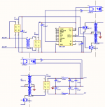
SMPS design sketch
Hello to everyone!
First off, I'm not experienced in SMPS design, but I'm very willing to learn. Even though my goal is to design and build a high power (500W+) supply, I want to start low, and work my way up. My main design principle is KISS (keep it simple, stupid), therefore I present to you one of my preliminary sketches. The whole thing is built around a SG3525 controller, with a conventional power supply in front of it. I am considering using the BP5041 (220VAC/12V 100mA) integrated converter from ROHM (not sure if it will cope with the current demands). I’m not sure whether I need a FET driver (can the SG3525 drive the FETs on it’s own?).
A problem I haven't found a solution for yet is what kind of filter is needed after the power transformer.
Well, as I’ve said before, this is only a sketch, and I’m very open to suggestions, comments and corrections, and every piece of advice tossed my way will be greatly appreciated. I'm hoping that my project can materialize soon, with the help of this forum.
Cheers!
P.S. oh, yeah... there are resistors between the controller's outputs and the FETs... you just can't see them 🙂
Attachments
Re: SMPS design sketch
Using the KISS method to approach any design is good. I think you are starting off with a difficult design. Look at what Eva did to get a great very practical and efficient SMPS in early posts in this thread. That design probably took a good bit of effort. For 500 Watts+ or any design for that matter, I would not try to re-invent the wheel, but use a very similar approach. Find some schematics on a 300 Watt+ PC SMPS to get more understanding of a real working SMPS. Avoid using opto-couplers. You can find some very good application notes to read at www.ti.com, following the power management link. Study both the data sheets and application notes on several of the PWMs. Look at current and voltage mode PWMs. Since you need transformers and inductors, go to the Mag Inc., and Ferroxcube websites and download their transformer and inductor design application notes. Get some of the basic understanding behind you, first. You will have to make your own PCB or create the layout and Gerber files. You can attach a Gerber file to an email and send it to a PCB manufacturer and have nice PCBs delivered possibly, depending on your location. Most PCB manufacturers will give you a price quote based on the Gerber file. You may already know how to make your own PCBs, but creating the layout for a medium to high power SMPS requires some very good analog layout skills.
sstoiana said:First off, I'm not experienced in SMPS design, but I'm very willing to learn. Even though my goal is to design and build a high power (500W+) supply, I want to start low, and work my way up. My main design principle is KISS (keep it simple, stupid), therefore I present to you one of my preliminary sketches. The whole thing is built around a SG3525 controller, with a conventional power supply in front of it. I am considering using the BP5041 (220VAC/12V 100mA) integrated converter from ROHM (not sure if it will cope with the current demands). I’m not sure whether I need a FET driver (can the SG3525 drive the FETs on it’s own?).
A problem I haven't found a solution for yet is what kind of filter is needed after the power transformer.
Using the KISS method to approach any design is good. I think you are starting off with a difficult design. Look at what Eva did to get a great very practical and efficient SMPS in early posts in this thread. That design probably took a good bit of effort. For 500 Watts+ or any design for that matter, I would not try to re-invent the wheel, but use a very similar approach. Find some schematics on a 300 Watt+ PC SMPS to get more understanding of a real working SMPS. Avoid using opto-couplers. You can find some very good application notes to read at www.ti.com, following the power management link. Study both the data sheets and application notes on several of the PWMs. Look at current and voltage mode PWMs. Since you need transformers and inductors, go to the Mag Inc., and Ferroxcube websites and download their transformer and inductor design application notes. Get some of the basic understanding behind you, first. You will have to make your own PCB or create the layout and Gerber files. You can attach a Gerber file to an email and send it to a PCB manufacturer and have nice PCBs delivered possibly, depending on your location. Most PCB manufacturers will give you a price quote based on the Gerber file. You may already know how to make your own PCBs, but creating the layout for a medium to high power SMPS requires some very good analog layout skills.
Some references :
This schematic shows a classic AT PC power supply with its self-oscillating auto-start feature and its separate current sense transformer for accurate current limiting [modern units sense the current through the base drive transformer in order to reduce costs]
This schematic shows a typical ATX PC power supply. Notice the primary side is no longer self oscillating and the current limiting is sensed on the base drive transformer. Notice also that the control circuit is powered from the standby separate supply [rudimentary flyback converter]
Old AT PSU topology, based on a half bridge that starts self oscillating until control circuit takes control, based on bipolar transistors and proportional current drive, tends to be very reliable. I still use an AT PSU in my computer and it's now 10 years old, 10 years working about 24hours/day and still no failures except noisy fans [replaced periodically]. This unit may actually live longer than me! 😀
http://www.qsl.net/xq2fod/Electron/PS40/PS40.html
And finally, this page has some info and explanations on a higher power unit [500W] using the same AT PSU topology. [Don't try to use these BUH transistors, I've tested it and they are very slow and expensive]
In the design of these kind of SMPS I think there are three tricky parts :
- Designing transformers to have low leakage inductance and to operate the cores at high magnetic fluxes but not enough to saturate it
- Designing output filter and frequency compensation of the voltage/current control loops to make them stable with the maximum permisible amount of feedback
- Optimizing switching waveforms for minimum ringing, low switching losses and no more dI/dt or dV/dt transients than required for operation
Then comes EMI reduction and filtering but this is a topic by itself Anyway, non-overlapped switching with bipolars and thorough a coupling transformer with some leakage inductance tends to generate much lower EMI than direct MOSFET-diode hard-switching
An externally hosted image should be here but it was not working when we last tested it.
This schematic shows a classic AT PC power supply with its self-oscillating auto-start feature and its separate current sense transformer for accurate current limiting [modern units sense the current through the base drive transformer in order to reduce costs]
An externally hosted image should be here but it was not working when we last tested it.
This schematic shows a typical ATX PC power supply. Notice the primary side is no longer self oscillating and the current limiting is sensed on the base drive transformer. Notice also that the control circuit is powered from the standby separate supply [rudimentary flyback converter]
Old AT PSU topology, based on a half bridge that starts self oscillating until control circuit takes control, based on bipolar transistors and proportional current drive, tends to be very reliable. I still use an AT PSU in my computer and it's now 10 years old, 10 years working about 24hours/day and still no failures except noisy fans [replaced periodically]. This unit may actually live longer than me! 😀
http://www.qsl.net/xq2fod/Electron/PS40/PS40.html
And finally, this page has some info and explanations on a higher power unit [500W] using the same AT PSU topology. [Don't try to use these BUH transistors, I've tested it and they are very slow and expensive]
In the design of these kind of SMPS I think there are three tricky parts :
- Designing transformers to have low leakage inductance and to operate the cores at high magnetic fluxes but not enough to saturate it
- Designing output filter and frequency compensation of the voltage/current control loops to make them stable with the maximum permisible amount of feedback
- Optimizing switching waveforms for minimum ringing, low switching losses and no more dI/dt or dV/dt transients than required for operation
Then comes EMI reduction and filtering but this is a topic by itself Anyway, non-overlapped switching with bipolars and thorough a coupling transformer with some leakage inductance tends to generate much lower EMI than direct MOSFET-diode hard-switching
taking notes
Ok! Very interesting links/schematics/hints/ideas... etc etc
Some things I've noticed so far :
a) low switching frequency = fast switching (FETs) is not needed = I can (should) use BJTs = low EMI
b) the controller IC should be on the low voltage side of the SMPS isolated using transformers (base drive tr, current sense tr) and powered using a low power transformer isolated switcher or a 50Hz transformer/conventional psu. These points being taken I'll post a revised sketch in a few hours.
Wow
Hi Eva!
I am quite impressed of your MJE 13009.
And also of your design!
I am not directly related to SMPS, especially not
PC-SMPS.....
And somehow my BJTs never were as good as yours.
Storage times I found at Ic/Ib=-4 :
XX13007 of various well known Semi-manufactures were
coming around 3µs and rise and fall times of the current were around 200ns to 400ns.
A Chinese low cost product was already at Ts=5us, but
except that fine.
The Chinese 13009 came with Ts=10us(!!!), but undestroyable 😀 ...
Not as outstanding as your MJ13009.
Self resonant topology:
Up to now nobody cares about THD of the mains current or
detailed harmonics in Computer SMPS. But I feel this may come.
If I am right this is also already in IEC-discussion for entertainment
electronics.... I am surprised that I do not hear anything about this here, or am tricked by wrong informations?
From this side I like PFC-Controllers-Chips + MOSFETS
in boost or flyback configurations... not the lowest cost solution, but still reasonable.... and of course a 1kW flyback
will not make much fun, except you are a transformer- and
snubber-GOD....
BJTs would be hard to drive from such Chips.
But if you have a constant load you may succed in a self resonant
design with some charge pump for correcting the input harmonics.
Or if you want to make it simple, you could use some
2C3D-Circuit behind the rectifier, popular in Asia.
Simple 2C3D-circuits typically result in a THD around 40% and a PF around 0.9.
Unfortunately the 2C3D circuit delivers a voltage that modulates
between peak value of mains and 50% of that.
I am not sure if selfresonant topologies will give proper
results with that.
Cheers and hoping that you are not in Madrid!!!!
🙁 🙁 🙁 🙁
Markus
Some reference from IR.
http://www.irf.com/technical-info/an998/an-998p1.htm
They call the 2C3D-circuitry different: valley fill passive PFC circuit.
I think checking through GOOGLE with the following key words
will give a lot interesting papers:
PFC, valley fill, charge pump, passive PFC etc.....
http://www.irf.com/technical-info/an998/an-998p1.htm
They call the 2C3D-circuitry different: valley fill passive PFC circuit.
I think checking through GOOGLE with the following key words
will give a lot interesting papers:
PFC, valley fill, charge pump, passive PFC etc.....
- Status
- Not open for further replies.
- Home
- Amplifiers
- Class D
- Line-powered SMPS for Power Amp?