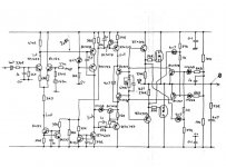
I came across an old tread in the archive about the encapsulated amps made by Les Sage in the UK around 1990. They were supposed to be Class A in terms of Sliding bias (non-switching) rather than the pointless but easy 50% bias most people use. Anyway, I unpotted one of his SUPERMOS amps and here is the circuit. It's not very impressive. Les is no longer alive so he can't answer for his claims...pity. See attached pic. regards Andy.
Attachments
Hi Andy,
Thanks for posting the circuit - I guess this was a SuperMOS 1 module - not SuperMos II, do you have details of the SuperMOS II?
I had a pair off SuperMOS II modules - however Sage Audio mounted the 3 pairs of output devices DIRECTLY to the heatsink module WITHOUT insulators. The anodising broke down in a short time and both modules failed...
So much for the claim of "No Capacitor" sound!
John
The Superamp had the '1' added when the bigger version was released.
I never bought a SuperMOS II
I've attached the datasheet to clarify the claims made for this design. (2x tif files in a ZIP. JPGs were too big if readable)
> So much for the claim of "No Capacitor" sound!
Also, so much for...
"Complex multiple nested compensation loops"
"low overall negative feedback"
"non-switching" ... etc
regards
Andy
Attachments
Andy,
Can you see ANY nested FB loops?
I thought it had no "Single Pole Compensation" - Er so whats the function of the 12pF Cap?
ARE you SURE this is the correct Schematic of SuperMOS - Sage Audio claimed 2 pairs of output devices - or did you not add them for clarity...
If true - it would seem that all the claims are false... ???
Does and body have a SuperMOS II module - I would be interested in buying and "De-Potting" the module...
John
Yes it's the right circuit. only 2 O/P devices. I bought them new and put them in a 3U rack box with separate 625VA toroidals (225VA would have been fine!) One module overheated and went BANG at a party, 4R with no fan :-( , no thermal protection. So I disected them both. It took me 2 weeks to fully un-pot them using dichloromethane. I may even have the bits at home, will post a pic if I do. Pity I don't have one left or I could measure it on my R&S UPL.
You have the R&S UPL - there great little machines - I have a couple of UPD's - fully loaded - these R&S are so much better then the AP's for R&D work - I've only used my AP2 C++ twice since new!!
John
John
In the Sage Audio info. you posted above, it claims they applied for a patent on the "8 transistor constant current / constant VCE superlinear gain block" - however I could find no record of a patent application by Les Sage or Sage Audio - can anybody shed any more light on this patent claim?
John
John
Hi Andy
is it really never switching off or only provided no phase shift between current and voltage?
I wish I understood how it actually works and which part is doing what. It will take me some time I'm affraid😀 ... complicated
regards
is it really never switching off or only provided no phase shift between current and voltage?
I wish I understood how it actually works and which part is doing what. It will take me some time I'm affraid😀 ... complicated
regards
Andy,
Are you sure that the 1nF Cap show connected between the output and the potential divider chain shound not have been connected to gound?
I don't understand this part of the circuit- it appears to be part of the output overcurrent protection (BC237B / BC307 / 4V7 Zeners + IN4148 etc) - or the "sliding Class A bias"?
John
> Are you sure that the 1nF Cap show connected between
> the output and the potential divider chain shound not
> have been connected to gound?
Very sure.
I now remember I threw away the bits 2 years ago :-(
Correct me if I'm wrong but I see it as:-
When output is s/c to 0V:-
When upper FET Vgs exceeds 4V7 ( the lower zener) plus 0v7 (Vbe of upper BC237B) the BC237B switches on and clamps the drive to the FET. Say around 5V4 Vgs
When output is NOT s/c to 0V:-
The 1N4148 adds a current drain path to a mid-rail pot-down. The 1K from the lower zener will need to supply more current before if can get to Vbe of the upper 327. The V(1K) adds to the existing 5V4 limit, so more than 5V4 Vgs allowed if output is NOT s/c.
At HF, the 1n will pull the mid-rail pot dynamically to follow the output, so reducing its function of leaking current away from the Vgs limiter. So Vgs MAX at HF may revert to 5V4 max even if output is UNLOADED.
Hi Andy,
I can't believe we've both done this at the same time, but last week I de-potted a Supermos-1 module myself, using the rather less elegant hammer-and-chisel method(!).
I don't understand the circuit as well as you, but I'll attach my first attempt at it anyway. It is very similar to that of your Supermos module, but there are certainly some differences. Some of these may be errors in my "reverse engineering", but I'm pretty confident about most of it.
Les Sage's claims for these modules were certainly "exaggerated", I note he said he used Holco 0.1% precision resistors, but all those pictured here are 10% carbon film types...
Also attached are a couple of pics of the module, for those that have asked. I've got lots more if anyone is interested.
Cheers,
Brian.
Pics: (click the thumbnails for full-sized images)
Circuit:
I can't believe we've both done this at the same time, but last week I de-potted a Supermos-1 module myself, using the rather less elegant hammer-and-chisel method(!).
I don't understand the circuit as well as you, but I'll attach my first attempt at it anyway. It is very similar to that of your Supermos module, but there are certainly some differences. Some of these may be errors in my "reverse engineering", but I'm pretty confident about most of it.
Les Sage's claims for these modules were certainly "exaggerated", I note he said he used Holco 0.1% precision resistors, but all those pictured here are 10% carbon film types...
Also attached are a couple of pics of the module, for those that have asked. I've got lots more if anyone is interested.
Cheers,
Brian.
Pics: (click the thumbnails for full-sized images)
An externally hosted image should be here but it was not working when we last tested it.
An externally hosted image should be here but it was not working when we last tested it.
Circuit:
An externally hosted image should be here but it was not working when we last tested it.
Brian
Nice work!
The build looks just the same.
It seems the 'Supermos1' is a redesign, reduced component configuration compared to my Supermos.
* No filter caps on your current sources
* Your TR10 is not paired in a cascode configuration.
* Different Vbe multiplier but still no sign of anything that would prevent either FET from switching off.
* Your 2 stage Vgs limiter uses a more familiar configuration.
Are you sure that D3/4 are not zeners (would be in reversed polarity to that shown) ?
I found my zener diodes by snipping one end & using a supply 6V(?) with 470R(?) in series to find the zener voltage.
I wonder why he needed to help the output to center using the two 1K resistors.
> I note he said he used Holco 0.1% precision resistors, but
> all those pictured here are 10% carbon film types...
Same on mine. And what about those awful radial electrolytics!
'tis a pity he's not around to answer a few questions.....
regards
Andy
D3/4 could very well be zeners, unfortunately the diodes were the only components to be totally destroyed in my heavy-handed de-pot (glass does not withstand impact well!) so I can't test them. I'm not even sure about the orientation, it was just a "best guess" while drawing the schematic, without really thinking about how it worked.
I think by comparing my schematic to yours I should be able to get closer to the true circuit. The Supermos1 looked like the PCB had little to do with the actual circuit, as there were far more unused pads than used ones, and loads of components directly soldered to one-another above the PCB. I guess the one original Superamp PCB might have been re-used up to the Supermos2?
I guess you found that the output FETs had their numbers sanded off as well? I think the "custom output transistors" was another of Les Sage's little white lies!
Cheers for the info anyway, I wish I understood the output stage a little better, but analogue electronics has never really been my forte.
I might stick the design into SPICE and see if I can understand what's happening - I think this might just re-kindle my interest in all things audio...
Regards,
Brian.
Brian
> ...there were far more unused pads than used ones, and
> loads of components directly soldered to one-another
> above the PCB.
Same on mine too. I assumed they were the standard FETs everyone used. J50 ??
A good space saving method though, especially as there were no surface mount components available.
> I guess you found that the output FETs had their numbers
> sanded off as well? I think the "custom output transistors"
> was another of Les Sage's little white lies!
Yep. Reckon so.
I was always suspicious of that one. You need a lot of money to get custom devices. And WHY.... ?
You don't need matched devices. The gently differing transfer functions of N & P ch devices is easily straightened by minimal local NFB, and are as nothing compared to the horrendous effect when one device reaches cut-off. ie: when ouput has moved about +/-50mA from steady state. ( 20mW @ 8R)
I wish someone would appear with a Supermos 2 circuit.
I could do with a good laugh 🙂
I think that was where he first mentioned the 'parabolic transfer function output driver' he had perfected !
PS: Your lower FET (TR2) needs to be flipped - Source up, drain down.
regards
Andy
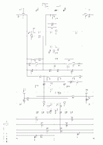
SuperMos 500 Diagram For Analysis
Hiya,
I have a supermos 500 circuit diagram that was drawn up from a de-potted failed SuperMos 500s in the mid 90s. I'd be intersted in what people have to say about this one. I can't believe people have suddenly started de-potting these after all these years 🙂 The SuperMos 500 was the daddy of all the SuperMos amps, but was about as reliable as the rest of them :-(
Les Sage always made big claims about his amps, but the acutual electronics never quite lived up to the claims.
I had a plan to build some of these years ago and my mate even came up with an improved circuit (the 'Onion' SuperMos500). I think one prototype was made but the 'dynamic' biasing never worked and the pan was to replace this with a conventional biasing ciruit... but never got around to it. I have schematics adn PCB layouts somwhere if any one is interested.
Cheers
N.
Attachments
Hi eclnj,
I'd be very interested to see the SuperMOS 500 circuit, but your attached GIF is unreadable! Could you attach a higher resolution image please? (might have to be a jpg to get under the file-size limit here).
Cheers,
Brian.
I'd be very interested to see the SuperMOS 500 circuit, but your attached GIF is unreadable! Could you attach a higher resolution image please? (might have to be a jpg to get under the file-size limit here).
Cheers,
Brian.
Thank you guys, one more myth is destroyed...
hate it also, only good for production lineI've only used my AP2 C++ twice
Hi eclnj,
FYI, my JPG picture at the start of this thread was 1000x742x16M colours and was 85kb file size.
Am looking forward to seeing your circuit.
regards
Andy.
FYI, my JPG picture at the start of this thread was 1000x742x16M colours and was 85kb file size.
Am looking forward to seeing your circuit.
regards
Andy.
SuperMos 500 Diagram For Analysis
.png files seem to do the trick ~50KB each. JPGs were still massive as the originals are 1500 * 2000 pixels! Resizing seems to make them unreadable. Zooming in 4 or 5 times seems to make them readable... The bit you can see 🙂 I can't remember how I printed them now, it was a long time ago.
Damn, I can't attach them as the image size limit is 1000 * 1000 pixels :-(
Bear with me on this one....
The 'Onion' version was modified from the original....
"There are slight changes to the original circuit
1) the input devices are now identical but with uequal base resistances to allow the DC restoration scheme to work
2) the cascode improves power supply rejection and allows higher Hfe trasistors at the input so the input impedance moves from 8K to 24k
3) an extra zener diode allows improved power supply rejection at the current source employing the BF858
4) The Hitachi MOSFETs are 'suitable' devices it has been impossible to determine what the originals were. They will have to be matched and may affect the frequency compensataion."
Please let me know what you think
Cheers
N.
- Status
- Not open for further replies.
- Home
- Amplifiers
- Solid State
- Les Sage amp circuit here for analysis