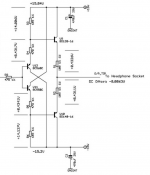
I have a question about the BD139 & BD140 output devices in the Lehmann buffer circuit below.
The schematic calls for the BD139 & BD140-16 devices which have the highest hFE.
What happens if you substitute the lower hFE devices like the BD139 & BD140-6 or -10?
Thank you...
The schematic calls for the BD139 & BD140-16 devices which have the highest hFE.
What happens if you substitute the lower hFE devices like the BD139 & BD140-6 or -10?
Thank you...
Attachments
I would imagine that you would see a slight increase in distortion at higher output levels when driving lower impedance loads.
I was concerned of saturating or "overloading" the output transistors since the BC transistors are also the highest hFE "C" grade devices.
Hi,
the BC drivers are biased just under 10mA, which is quite a lot.
even if the BDs were runnung on 100mA of bias current they´d require less than 1mA of Base current.
So nothing to worry about.
THD may rise a bit with lower hfe BDs but on a rather negligable niveau.
This Buffer is the second simplest form of an Diamond Buffer.
The drivers run on ~9mA bias, the outputs on 40-45mA.
Heat power loss of the BCs is ~140mW and ~550mW for the BDs.
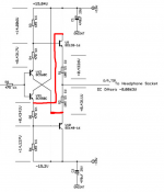
THD improves when You connect V12´s collector to V10´s emitter and V9´s collector to V11´s emitter.
Also the driver´s losses reduce considerably down to ~10mW, allowing for SMDs.
The BD´s power losses incerease though by ~100mW to 650mW.
jauu
Calvin
the BC drivers are biased just under 10mA, which is quite a lot.
even if the BDs were runnung on 100mA of bias current they´d require less than 1mA of Base current.
So nothing to worry about.
THD may rise a bit with lower hfe BDs but on a rather negligable niveau.
This Buffer is the second simplest form of an Diamond Buffer.
The drivers run on ~9mA bias, the outputs on 40-45mA.
Heat power loss of the BCs is ~140mW and ~550mW for the BDs.
THD improves when You connect V12´s collector to V10´s emitter and V9´s collector to V11´s emitter.
Also the driver´s losses reduce considerably down to ~10mW, allowing for SMDs.
The BD´s power losses incerease though by ~100mW to 650mW.
jauu
Calvin

Hi,
not quite right, just one half 😉
Follow the link to my website, bipolar Buffers and see Fig.5 and associated description
jauu
Calvin
not quite right, just one half 😉
Follow the link to my website, bipolar Buffers and see Fig.5 and associated description
jauu
Calvin
Bootstrapping. Not as good as CCS but simple and with lower voltage drop over the output transistors.Is there anything else you would change about this buffer to improve its performance?
Calvin said:not quite right, just one half
He preciselly followed your instructions. He didn't notice small typing error 😀
Calvin said:THD improves when You connect V12´s collector to V10´s emitter and V9´s collector to V11´s emitter.
Should read: higher output voltage swing. Sorry for my bad English.lower voltage drop over the output transistors.
Should read: higher output voltage swing. Sorry for my bad English.
No problem...thanks for the input.
Ive been using this circuit and i like it. However id like to lower the output bias a tad bit. Do i decrease the 1k5 ohms or else?
Increasing R3 & R6 will decrease output transistors bias, which is also determined with R4 & R5. So, options are to decrease R4 & R5 to 39R or to increase R3 & R6 to 2K2.
Base current for these transistors comes through the 1k5 resistors. So when the output swings close to the supply rail, voltage across these resistors is reduced, and available base current is reduced, which reduces output current capability. So, using lower hFe transistors will reduce output voltage swing in a low impedance load. You can calculate by how much depending on load impedance and therefore output current. With 600 ohms headphones, the effect is likely to be absolutely negligible.What happens if you substitute the lower hFE devices like the BD139 & BD140-6 or -10?
- Home
- Source & Line
- Analog Line Level
- "Lehmann" Buffer Output Transistors.