You folks are quite right about substituting. Use what works and is easily available near you. That the parts in question are obsolete re-begins the rumor that has continued over the past ten years or so.
Even Prof. Leach mentions this in years past.
Those of us who live near Silicon Valley are spoiled.
Reputable sellers are not that hard to find. Most will ship to anywhere.
Never had a problem with fakes from any US source unlike other parts of the world where fakes seem to be quite common. Minor irritation to ship stuff to family in Makati. Have to make a trip to the local LBC store and do some paperwork. Put some Spam in the box and everyone is happy.
Regards
AndrewT said:Hi Tony,
are you recommending that To92 run at 16% to 17% of maximum rating or simply confirming the existing design?
What is your % dissipation recomendation for the VAS, predriver and driver?
Anyone else with a view on max quiescent dissipation?
i suggest you read up on the original article by Leach published in the AUDIO magazine in 1980.
way i understood it, Leach chose 4mA tail current as optimum value, consistent with gain and noise and of course quiscient dissippation. that he linearised the stage by reducing stage transconductance thru use of emmiter degeneration resistors. nowadays, this thinking has changed, AKSA for example uses less than a 1mA tail current if i am not mistaken.
as for VAS, a quiscient dissipation of about 400mW per device, and the drivers are operated class A, while the output at class AB. the output transistors are not really cut-off due to idle bias currrent.
i emailed Dr. Leach once and asked him if i can adapt the feedforward scheme to the super leach amp, and he replied, "I wouldn't change a thing."
can't blame him, i have built several of these super leach amps, with different transistor compliments and rail voltages and the results were always the same. those who heard the amps play liked what they heard.😀
Minor irritation to ship stuff to family in Makati.
are you by any chance Pinoy?😀
The Boards are about 108 x 325 mm
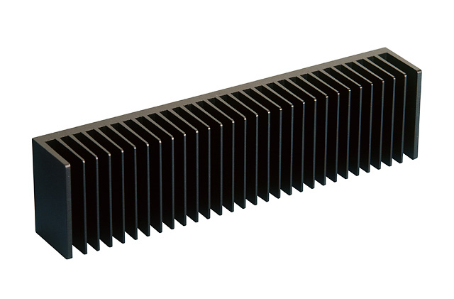
I have suggested a heatsink from conrad.
I would still like some more input about footprints for the different parts, I have explained that I will not work on the layout untill somebody steps up and help me deside what parts to make room for.
Im thinking of redoing the whole board design right now, with the parts I already have on board. This board will not be a GB board as my componets are hopeless compared to audiophile stuff and the PBC will have 4 layers.
Btw, why does nobody come forward and help to get this thing running???
\Jens
I nominate sir Tony... whose a very competent diy'ers... 😎
Go for it Tony
glad to see locally available parts in jens boards...
Go for it Tony
glad to see locally available parts in jens boards...
i am going on an overseas work at the Zakhalin islands from 17Feb. onwards and may be incomunicado for a while, but i sure would like to join the group buy if and when it pushes thru.
jens,
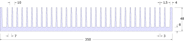
the conrad heatsink 105mm x 400mm looks good, however, my choice is 2 x 105mm x 250mm though.
any chance providing around 2mm more separation between T13/T13A, T9/T9A, T8/T8A, T12/T12A? this is to have more choices in using plastic transistors.
thanks
jens,
the conrad heatsink 105mm x 400mm looks good, however, my choice is 2 x 105mm x 250mm though.
any chance providing around 2mm more separation between T13/T13A, T9/T9A, T8/T8A, T12/T12A? this is to have more choices in using plastic transistors.
thanks
Hi,
a 105mm high heatsink puts the power transistors right at the edges of the sink. This is poor for heat transfer efficiency. The heat is effectively flowing in one direction i.e. towrds the middle of the sink. Both the BJT data and the sink data will over estimate the dissipation ability of this ill advised combination. I cannot advise how much error will result but I would not be surprised at a figure approaching -30%.
I would recommend the sink extend at least 10mm above and below the top and bottom edges of the power BJTs, giving a minimum height of 120mm if the 100mm wide PCB is finalised.
Personally I would use 140mm to 150mm high sinks for a 100mm PCB.

An idea for the PCB
Hi Jens
Have followed this thread with interests. I really appreciate your effort designing such an
amp project and your thoughts of sharing this with us DIY Hi-Fi enthusiasts 😉
I also love the Conrads heat sinks and I plan to buy 10pcs M-35-151 (look at my GB info.)
Somebody interested?
Regarding your further design with the PCB: could be beneficial to design the PCB with an option that makes it possible to cut the long main board in two parts (driver board + output devices). Reason for that is the long PCB will not fit in all the chassis (old chassis as well as new ones) that could be used by the DIYs
This option could be done by designing the main board in such a way that it contains a cutting zone, a space between the driver board area and the output device area where you can make a cut. This small space/zone could also be fitted with pre-drilled solder eyes for cable/conector connections between the two boards. This gives the DIYs the possibility to use different power device boards (e.g. their own design for other type of output devices). Just an idea.
BTW no matter how the ending design will look like. I want to buy at least two boards for my purpose (possibly it will be 4) and I shall use the Conrads.
Looking forward to buy these BCBs from you Jens,
Regards
What source would I look to in order to begin applying component values into the schematic provided by Jens?
I'm interested in this as well. I need a little guidance in order to do the legwork to move this along.
Also, what range of output wattage will we expect to see from this rendition?
Thanks.
I'm interested in this as well. I need a little guidance in order to do the legwork to move this along.
Also, what range of output wattage will we expect to see from this rendition?
Thanks.
Tony said:nice idea😀
i am good for about 6 boards either way.
Hi, sir tony, how are you? How' s your work there in Russia?
with rails of +/-85volts, that'll give you 250 watts per channel depending on how stiff your power supply is.
the parts are much like the ones for the small leach amp, you can start from there.
the parts are much like the ones for the small leach amp, you can start from there.
BlackMTX said:
Hi, sir tony, how are you? How' s your work there in Russia?
sweating it out in the snow.
😀
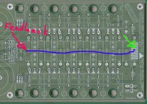
Just checked the pcb.
First of all: A very nice looking pcb, indeed.

My little remark is that you have forgotten to include _all_ transistors in the feedback. It's possible that this is of minor importance but possibly you could reduce distortion and the output impedance. My patch is easy to test if it means anything. A basic rule I think everyone can agree on is to include _everything_ in side the feedback loop. I know the copper was thick but the resistance isn't zero.
My patch is to move the point of feedback. See the blue line. It's possible that it's needed to shunt this blue line with 100 pF - 1 nF at the original feedback point.
First of all: A very nice looking pcb, indeed.
My little remark is that you have forgotten to include _all_ transistors in the feedback. It's possible that this is of minor importance but possibly you could reduce distortion and the output impedance. My patch is easy to test if it means anything. A basic rule I think everyone can agree on is to include _everything_ in side the feedback loop. I know the copper was thick but the resistance isn't zero.
My patch is to move the point of feedback. See the blue line. It's possible that it's needed to shunt this blue line with 100 pF - 1 nF at the original feedback point.
Attachments
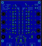
That is not a super amp PCB...
This is my first factory made PCB for the extended Leach amp the layout is more than two years old and the discussion about take off point for the NFB is about the same age.
The PCB in GB for the redesigned Leach amp PCB was changed so that the FB was taken directly at the output inductor.....
\Jens
Attachments
- Status
- Not open for further replies.
- Home
- Amplifiers
- Solid State
- Leach Super Amp Pcb Re-Design (LSAPRD)