I have been working on the second channel of a leach amp. I have gotten the first channel working alright, but now I have an issue with the second channel.
When running the diagnostic tests at +-20V rails, the output has a huge DC offset; 2.5V with input grounded, and somewhere around 8-10V with input floating. I'm really at a loss of where to look in the circuit for errors.
When I first started up, there was a current limit on the negative rail, and I determined that there was a solder bridge between - rail and ground, on the input side of the 82ohm resistor. Could that have caused other failures?
I've looked at the Leak Delta stereo 70 schematic, and the Leak Stereo 30 schematic. I'm sorry, I don't believe you are talking about one of these. Specific model information would help.
In solid state amps, trouble in the output transistor stages (exhibits DC offset on speaker) often damages things driving them, sometimes one level back, sometimes two or three levels back. You frequently have to check parts all through the amp. It is a bad message, but has been true one on my latest project. Transistors, resistors, PCB lands, Even little rice grain sized ceramic caps, that look perfect, but have stopped doing anything useful. Good hunting for the bad parts.
In solid state amps, trouble in the output transistor stages (exhibits DC offset on speaker) often damages things driving them, sometimes one level back, sometimes two or three levels back. You frequently have to check parts all through the amp. It is a bad message, but has been true one on my latest project. Transistors, resistors, PCB lands, Even little rice grain sized ceramic caps, that look perfect, but have stopped doing anything useful. Good hunting for the bad parts.
I have been working on the second channel of a leach amp. I have gotten the first channel working alright, but now I have an issue with the second channel.
When running the diagnostic tests at +-20V rails, the output has a huge DC offset; 2.5V with input grounded, and somewhere around 8-10V with input floating. I'm really at a loss of where to look in the circuit for errors.
When I first started up, there was a current limit on the negative rail, and I determined that there was a solder bridge between - rail and ground, on the input side of the 82ohm resistor. Could that have caused other failures?
check for wiring errors looking at the working channel for comparison....be patient and take your time....do not rush things....
It's the Leach amp, then the 82 ohm resistor will definitely burn if the frontend supply end is shorted to ground. This condition connects the 82 ohm resistor across 56 volts.
Gajanan Phadte
Gajanan Phadte
I've looked at the Leak Delta stereo 70 schematic, and the Leak Stereo 30 schematic. I'm sorry, I don't believe you... QUOTE]
OP is referring to The LEACH amp.
Gajanan Phadte
compare voltage between the two channels.
That could help identify where the error starts to occur.
That could help identify where the error starts to occur.
Okay, thanks for the replies so far. Yes, it is the LEACH amp, not Leak.
I have done some testing today. I never connected to +-50V rails. I have only been working from +-20V bench supply.
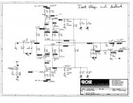
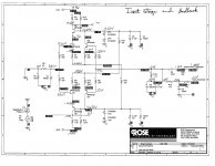
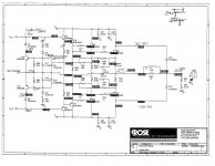
Anyway, I have attached three files. It is my PSpice simulation of the Leach amp running on 20V rails. I have written in pencil the measurements of the DC bias points that I took today.
The voltage after the input low-pass filter does not seem right at all to me, but I'm not sure if it's a problem with the filter itself or the following BJTs.
When I created the first channel, it worked at +-20V rails, just with clipped output. But this channel doesn't get signal past the first stage.
I have done some testing today. I never connected to +-50V rails. I have only been working from +-20V bench supply.
Anyway, I have attached three files. It is my PSpice simulation of the Leach amp running on 20V rails. I have written in pencil the measurements of the DC bias points that I took today.
The voltage after the input low-pass filter does not seem right at all to me, but I'm not sure if it's a problem with the filter itself or the following BJTs.
When I created the first channel, it worked at +-20V rails, just with clipped output. But this channel doesn't get signal past the first stage.
Attachments

2.2Vdc at the grounded input tells you you have a current of 2.2mA flowing out of the base connection.
The Vdrop of r5 tells you the excessive base current is coming from Q3.
Looks like a broken transistor.
As a double check Vbe ~+0.05Vdc whereas it should be ~-600mVdc for a PNP.
The Vdrop of r5 tells you the excessive base current is coming from Q3.
Looks like a broken transistor.
As a double check Vbe ~+0.05Vdc whereas it should be ~-600mVdc for a PNP.
Andrew, thanks for taking a look. I have re-run my pspice simulation with a 250ohm resistor from base to emitter of Q3, and I get bias points that are roughly similar to everything else I have measured.
It seems that the BJTs on the Leach amp are particularly susceptible to damage during construction. Also, the PCBs I am using were single-sided milled out here at school, and it's fairly easy to bridge traces. So that is an issue.
I will double check a few more things and then probably replace Q3 and report back my results.
no more so than any other equipment using semiconductors..........It seems that the BJTs on the Leach amp are particularly susceptible to damage during construction..........
So NO !
if you matched Q3 to it's three mates then you will have to rematch your four transistors. It's in the Leach build details.
Right. I have four spares I believe, so I was planning on determining beta for those four, and getting one closest to the three in the circuit already.
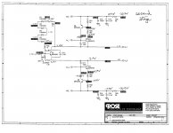
Okay, I have replaced Q3. Some of the q points are better, but signal is still not being passed to output.
I have attached similar measurements as before. Any advice would be greatly appreciated!
I have attached similar measurements as before. Any advice would be greatly appreciated!
Attachments
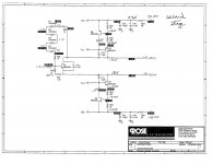
0.37 volts output offset is unacceptable....must be below 0.1volts, closer to 0 is better...
you need the match your input trannies for hFE, the npn's and the pnp's..
you input ltp is cutoff at such low voltage.....why not use the proper voltages....you can temporarily replace the fuses with 10ohm 1/4 watt resistors, one each for the positive and negative rail....if everything this will prevent loss of your output trannies, they will get burned out instead...
you can then use those resistors to adjust your bias current....i have been building leach amps for the last 20 years, the leach amp is very good....
0.37 volts output offset is unacceptable....must be below 0.1volts, closer to 0 is better...
you need the match your input trannies for hFE, the npn's and the pnp's..
I did match the input transistors. Is this large offset due to the fact that the rails aren't at full voltage? I tested the other channel at +-20V rails, and signal was passed all the way through, albeit clipped. But the signal doesn't get passed through on this channel. I still think something is blown...
2.2Vdc at the grounded input tells you you have a current of 2.2mA flowing out of the base connection.
The Vdrop of r5 tells you the excessive base current is coming from Q3.
Looks like a broken transistor.
As a double check Vbe ~+0.05Vdc whereas it should be ~-600mVdc for a PNP.
or a wrong polarity transistor(base emitter is forward biased, that is why you have such voltage at input)....need to make sure that trannies are inserted correctly.......
I did match the input transistors. Is this large offset due to the fact that the rails aren't at full voltage? I tested the other channel at +-20V rails, and signal was passed all the way through, albeit clipped. But the signal doesn't get passed through on this channel. I still think something is blown...
yes that is possible, but i think you got the biasing right or else you could have blown the output trannies....
so match your input ltp trannies, and check your trannies for insertion errors...
or a wrong polarity transistor(base emitter is forward biased, that is why you have such voltage at input)....need to make sure that trannies are inserted correctly.......
No, Q3 was indeed blown. I replaced that, and the scans I just posted today are the new dc points I measured.
There originally was a solder bridge between V- and GND, which accounts for why q3 died. But something else is bad, and I'm not sure what it is.
can you post actual pictures? time to test at full voltage using the 10ohm current limiting resistors...if you have a variac, that would even be better...
- Status
- Not open for further replies.
- Home
- Amplifiers
- Solid State
- Leach amp troubleshooting