Hi stinius,
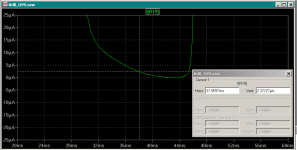
It has been 28 days since I posted the requested files. It looks like no one is going to use the models you posted, so I learned enough about LTspice to run the file Andy_C posted earlier. I have attached my results. I ran the file as posted by Andy, then just for fun, I ran it again with the bias resistor changed from Rbias to 4200 ohms. That is what the text in the lower left indicates the value Rbias is. I was not the least bit surprised to see that if you zoom in on the wave form and do the math, it appears the transistors do not turn off. That is what I have claimed all along. What does surprise me is that changing the bias resistor from Rbias to 4200 ohm changed the results. Does anyone have an explanation for why this happens?
Hi Steve,
I just tried this out after receiving an email from another poster. There is no difference at all between using .param Rbias 4200 while specifying the resistor as {Rbias} versus specifying it directly as 4200. If there were, LTspice would be broken. I did try it myself.
It does make a difference where the marker is placed on the waveform. If it's in the middle of the approximately flat bottom portion of the trace, you get a few uA as shown in the PDF file you attached. This is shown in a blowup view in the attached graphic at 5 uA/div, 38msec into the sim, same as your PDF in post 138. Compare this with the PDF attachment of your post #138, which is at 30mA/div. That one shows 3.6uA in the data window at the lower right. So it looks like we're pretty close. Thanks for taking the time to do the LTspice simulation.
Edit: The reason the .param was in there is to optimize distortion per the earlier discussions. If you do this:
.step param Rbias list val1 val2 val3 val4
and do a sim with distortion, the LTspice error log file will contain the simulated distortion values for each of val1, val2, and so on.
Sorry for being so grouchy earlier.
Attachments
Last edited:
Oh, just one more thing. I was wondering why I was getting 2.3uA and you were getting 3.6uA at time 38 msec for the same simulation. In looking more closely at the PDF file of your post #138, I saw that you changed the emitter resistor value from my 0.22 Ohms to 0.1 Ohms. This changes the bias current in the output devices from 262.2mA to 347.5mA. The original 262.2mA was the one that minimized distortion per your earlier direction for bias adjustment. After making this change to the higher bias, I got extremely close to your 3.6uA value at 38 msec. Then the current went to a minimum of about 2uA, rather than going to zero as my plot above shows. Maybe it was this change, and not the 4200 Ohm replacement that made the difference?
Last edited:
I need to correct one thing I said earlier. I said I only ran the 4 ohm and 2 ohm sim in LTspice at 1K. The actual frequency I used was 20Hz.
Hi Andy,
That is a good thing. I probably didn't have the marker at the same point both times. For later runs, I zoomed in close and found the minimum by moving the marker slowly across the wave form.
I assumed that was why you had done that. No problem with the grouchy part. I was pretty abrasive myself back when we were in the original Krill thread.
I changed the emitter resistors to 0.1 ohm because that is what I used in my sims in Intusoft and that was what I had posted in post 127. With my sims in Intusoft, I got the lowest distortion at 202.8ma bias. I changed the bias resistor to get that value with LTspice. That value ended up being 882 ohm. I havent checked the distortion with LTspice yet. I will try to do that today if I have time. I think the small differences in results between Intusoft and LTspice can be attributed to the different models used in the two programs. The change in Rbias was probably made necessary by the use of different transistor for the bias transistors. Does that sound reasonable?
The fact that the results were that close, even with these differences, gives me more faith in the results that can be obtained with simulation.
Hi Andy,
I just tried this out after receiving an email from another poster. There is no difference at all between using .param Rbias 4200 while specifying the resistor as {Rbias} versus specifying it directly as 4200. If there were, LTspice would be broken. I did try it myself.
That is a good thing. I probably didn't have the marker at the same point both times. For later runs, I zoomed in close and found the minimum by moving the marker slowly across the wave form.
Edit: The reason the .param was in there is to optimize distortion per the earlier discussions. If you do this:
.step param Rbias list val1 val2 val3 val4
and do a sim with distortion, the LTspice error log file will contain the simulated distortion values for each of val1, val2, and so on.
Sorry for being so grouchy earlier.
I assumed that was why you had done that. No problem with the grouchy part. I was pretty abrasive myself back when we were in the original Krill thread.
Oh, just one more thing. I was wondering why I was getting 2.3uA and you were getting 3.6uA at time 38 msec for the same simulation. In looking more closely at the PDF file of your post #138, I saw that you changed the emitter resistor value from my 0.22 Ohms to 0.1 Ohms. This changes the bias current in the output devices from 262.2mA to 347.5mA. The original 262.2mA was the one that minimized distortion per your earlier direction for bias adjustment. After making this change to the higher bias, I got extremely close to your 3.6uA value at 38 msec. Then the current went to a minimum of about 2uA, rather than going to zero as my plot above shows. Maybe it was this change, and not the 4200 Ohm replacement that made the difference?
I changed the emitter resistors to 0.1 ohm because that is what I used in my sims in Intusoft and that was what I had posted in post 127. With my sims in Intusoft, I got the lowest distortion at 202.8ma bias. I changed the bias resistor to get that value with LTspice. That value ended up being 882 ohm. I havent checked the distortion with LTspice yet. I will try to do that today if I have time. I think the small differences in results between Intusoft and LTspice can be attributed to the different models used in the two programs. The change in Rbias was probably made necessary by the use of different transistor for the bias transistors. Does that sound reasonable?
The fact that the results were that close, even with these differences, gives me more faith in the results that can be obtained with simulation.
Hi all
Sorry to jump in late and sorry again if I'm just being thick, but ....
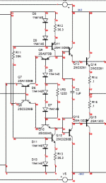
Ignoring for a moment the arguments about charge being sucked out of the output device's bases etc, what the heck is going on with Q7, Q8, Q9 and Q10?
As far as I can see, Q9 and Q10 are being driven at their collectors😕. E.g. Q8's emitter drives Q10's collector
For a minute there I thought maybe Q9 and Q10 are supposed to be running saturated, but a quick count of the Vbe voltage drops all round suggests not.
Can someone please explain what's going on there? (or if it was explained in some previous thread, just point me in the right direction)
Thanks - Godfrey
Sorry to jump in late and sorry again if I'm just being thick, but ....
Ignoring for a moment the arguments about charge being sucked out of the output device's bases etc, what the heck is going on with Q7, Q8, Q9 and Q10?
As far as I can see, Q9 and Q10 are being driven at their collectors😕. E.g. Q8's emitter drives Q10's collector
For a minute there I thought maybe Q9 and Q10 are supposed to be running saturated, but a quick count of the Vbe voltage drops all round suggests not.
Can someone please explain what's going on there? (or if it was explained in some previous thread, just point me in the right direction)
Thanks - Godfrey
Attachments
Last edited:
Hi all
Can someone please explain what's going on there? (or if it was explained in some previous thread, just point me in the right direction)
Thanks - Godfrey
Howdy Godfrey - and welcome to Krill-Asylum
Hugh Dean of Aspen Amps did a nice write-up of topology and it's available at Steve's site. Just click on the link provided in his threads. 😉
Dunlap Audio
Godfrey,
Well, it would not be an easy task for anyone to come up with a more nonlinear output stage configuration than this.Ignoring for a moment the arguments about charge being sucked out of the output device's bases etc, what the heck is going on with Q7, Q8, Q9 and Q10?
As far as I can see, Q9 and Q10 are being driven at their collectors. E.g. Q8's emitter drives Q10's collector
Godfrey,
Well, it would not be an easy task for anyone to come up with a more nonlinear output stage configuration than this.
I don't suppose you are willing to explain your opinion.
Lumba,
Well, it would not be an easy task for you to come up with a more credible explanation than this.
Hugh
Well, it would not be an easy task for you to come up with a more credible explanation than this.
Hugh
Steve,
as already stated, the "non-switch arrangement" does not do any good in any respect, therefore should be abandoned. As for the Darlington stage, the drivers should be class A biased and the output transistors should be reversed biased, because the drivers alone cannot shut off the base current of the output transistors, moreover, even a small leakage current causes disturbances (the cut-off problems will remain to some extent in any case).
Compared to the single device, the Darlington pair means larger distortion as a price of larger current gain, due to:
Double nonlinear base-emitter junctions
Doubled base-emitter voltage
Limited bandwidth
More phase shift
Slow switching speed (about three times longer turn-off time)
High saturation voltage
LTSpice hasn´t indicated this? Of course not. Being a particularly incompetent tool, it simply cannot, but maybe is an amusing toy for people having much time to waste.
Steve,
as already stated, the "non-switch arrangement" does not do any good in any respect
Hmm, as a cool running AB amp, for pro use it would seem to make sense
Fore hifi home use, maybe less advantage, or none
Or it may as a cool running classA
But we will see about that
I suppose any distortion could be measured fairly easy
Lumba
I do not use LTspice except to run the file that Andy posted.
The posted circuit has a bandwidth of over 1MegHz. There is one degree of phase shift at 97KHz.
You seem to frequently make statements criticizing other peoples circuits without any insight into how they operate. You don't like my circuit. That's fine with me, but you would be taken more seriously if you knew what you were talking about.
LTSpice hasn´t indicated this?
I do not use LTspice except to run the file that Andy posted.
Limited bandwidth
More phase shift
The posted circuit has a bandwidth of over 1MegHz. There is one degree of phase shift at 97KHz.
You seem to frequently make statements criticizing other peoples circuits without any insight into how they operate. You don't like my circuit. That's fine with me, but you would be taken more seriously if you knew what you were talking about.
In the idealized case crossover distortion has nothing to do with the output devices turning off. The logarithmic Vbe modulation between several amps and several micro amps is enough. I still don't get the fixation with "does the output device turn off".
Hi Scott,
Following up on what you said, what range of current change is enough for this to begin to be a significant source of distortion? I know that is a subjective point, but I'm not sure how else to word it.
Hi Scott,
Following up on what you said, what range of current change is enough for this to begin to be a significant source of distortion? I know that is a subjective point, but I'm not sure how else to word it.
It has to do with charge storage and speed of turn off/on coming in/out of deep quasi-saturation. Base currents go backwards, etc. None of this is dealt with in a simple look at things. A simple diamond output with no degeneration never shuts off in the ideal case just one side is X times more current and the other side is 1/X times smaller. I noticed the discussion has moved to 200 or 300 mA of bias, this is way outside of the original few mA. 20 or 30 mV across .1 Ohm is close to the optimum bias.
Most IC op-amps have fast enough output devices that both sides are operating in normal forward bias conditions as they approach crossover. Then the theoretical translinear Vbe equations predict the crossover distortion almost exactly. This may not be the case with low ft huge power transistors. Though the Vbe modulation is always there in addition.
EDIT - It has a lot to do with the device sourcing lots of current turrning off as well as the off device turning on.
Last edited:
BTW, by a "simple look at things" I meant that you can not explain the dynamic behavior by walking through the circuit point by point and applying basic Vbe, Ic, Ib, beta, etc. arguments. When you try to turn off a transistor that is hard on at amps you can and do sometimes get a negative base current while the Ic is still positive this will also depend on how fast things are moving. Neither the Ic = beta*Ib or the Vbe equation are totally valid in this region.
To what degree is this distortion measurable? What is the spectra like? This is what I was interested in finding more information on.
The 300ma was an error, and I caught and corrected it later. You are right about me having moved on to the 200ma bias and the lower value emitter resistors. As I have tried to say before, I planned all along to present my design as a work in progress. Start with the simplest amp that would work reliably and sound good while being stable under almost all conditions.
As for the 25ma bias that keeps getting repeated, I went back to look at that post. Here is what I said:
I never intended that to mean that 25ma was the optimum bias current, just an absolute minimum. At that time, I was still very new here. I was laboring under the illusion (and a lot of drugs) that this was a DIY site where not every reader would have access to a full test lab. I still believed that some here wanted a small measure of guidance in their projects. Had I known that I was addressing only seasoned professionals in the industry, I would certainly stated things differently.
I noticed the discussion has moved to 200 or 300 mA of bias, this is way outside of the original few mA. 20 or 30 mV across .1 Ohm is close to the optimum bias.
The 300ma was an error, and I caught and corrected it later. You are right about me having moved on to the 200ma bias and the lower value emitter resistors. As I have tried to say before, I planned all along to present my design as a work in progress. Start with the simplest amp that would work reliably and sound good while being stable under almost all conditions.
As for the 25ma bias that keeps getting repeated, I went back to look at that post. Here is what I said:
That is why I recommended using a distortion meter to set bias. If you do not have access to a distortion meter then set the idle current between 25 and 100mA. This will depend to a large extent on the transistors you use.
I never intended that to mean that 25ma was the optimum bias current, just an absolute minimum. At that time, I was still very new here. I was laboring under the illusion (and a lot of drugs) that this was a DIY site where not every reader would have access to a full test lab. I still believed that some here wanted a small measure of guidance in their projects. Had I known that I was addressing only seasoned professionals in the industry, I would certainly stated things differently.
Wouldn't we all, Steve. Be nice if the seasoned professionals were a little less sneering and answered their PMs.....
Hugh
Hugh
Thank's guys. If there is anything "sneering" in those two answers I must be missing something. After all I was asked a question, there simply is not an easy answer.
If there is any possible misinterpretation, or ambiguity, in forum posts, particularly in a difficult arena like electronics, the worst is almost always assumed.
Very great care is needed to make unambiguous, clear posts. It's difficult. Yes, your posts had seemed a bit sneering to me, given what has gone before and your abdication in the past to others on these matters, but your explanation just now shows you did not mean to patronise. Furthermore, your explanation was fairly clear.
My sincere apologies on the first issue; however, the PM issue remains, not so easy to misinterpret.
BTW, solely my criticism, not Steve. He has been above reproach in this long dissertation.
Hugh
Thank's guys. If there is anything "sneering" in those two answers I must be missing something. After all I was asked a question, there simply is not an easy answer.
I asked a question and you gave an answer. I was not aware of any sneering in your answer. I then ask another question, or perhaps the same question worded differently. I am sincere in my desire to learn to what degree this crossover distortion might negatively impact sound quality or measured performance.
I plead guilty to maybe being just a tad sarcastic in my comments about bias setting, but the figure of 25ma has been brought up repeatedly by others than just yourself. I hoped to settle that misunderstanding.
You are right about me having moved on to the 200ma bias and the lower value emitter resistors.
If so, could you expand (sorry if I missed something lately) how/why is Krill better than an triple EF output stage (like the Locanthi T), biased at the optimum (26mV across Re of 0.1mA = 260mA)?
Secondly, don't you think Re=0.1ohm is a little low for any practical implementation of a bipolar output stage (be it Krill or EF)?
- Status
- Not open for further replies.
- Home
- Amplifiers
- Solid State
- Krill - The Next Generation