Kolinummi concept for reducing crossover distortion implementable on Blameless
I decided to create a new thread to specifically discuss the Kolinummi error correcting output stage reviewed in this thread. The second page of the thread references Kolinummi and the Benchmark amplifier. Kolinummi provides references all the way back from the 1980s on amplifiers with error correcting output stages, so Benchmark may have a new implementation but it is not a new idea.
Kolinummi proposes taking the difference between the center of the drivers and the center of the output stage voltage and superimposing the opposite voltage on the input. The mechanism they use is to feed this back as a current through the VAS, but they use a somewhat unconventional VAS stage.
I first simulated this concept by imposing constraints in LTSpice and it was promising, so I went on to figure out how to practically implement it in a "Blameless" style amplifier. The implementation I developed was to take the error using a long tailed pair, and then inject the error current into the inverting input of a VBE multiplying voltage reference. The VBE multiplier is nominally at 2V, and can swing +/-1V to support error cancellation. The method works beautifully.
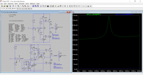
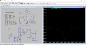
Attached is an LTSpice simulation comparing an emitter follower stage biased to 20mA and an error cancelling emitter follower stage. For the first plot, I made a current injection of -3A to +3A over 1 second to find the apparent output impedance versus current. For the second plot, I swept the input voltage from -10V to 10V over 1 second to find the voltage dependent gain.
I made similar analyses (not shown) for CFP and Renardson output stages, and they are not as attractive.
I hope this is useful to some. Let me know what you think. I added a capacitor across the LTP and the VBE multiplier to better control the inverting error amplifier impedance at high frequencies, but I don't normally see these elsewhere. I also used a CFP style VBE multiplier to improve its gain linearity, but a simple one may also be suitable with a slight change in resistance to adjust the gain.
I decided to create a new thread to specifically discuss the Kolinummi error correcting output stage reviewed in this thread. The second page of the thread references Kolinummi and the Benchmark amplifier. Kolinummi provides references all the way back from the 1980s on amplifiers with error correcting output stages, so Benchmark may have a new implementation but it is not a new idea.
Kolinummi proposes taking the difference between the center of the drivers and the center of the output stage voltage and superimposing the opposite voltage on the input. The mechanism they use is to feed this back as a current through the VAS, but they use a somewhat unconventional VAS stage.
I first simulated this concept by imposing constraints in LTSpice and it was promising, so I went on to figure out how to practically implement it in a "Blameless" style amplifier. The implementation I developed was to take the error using a long tailed pair, and then inject the error current into the inverting input of a VBE multiplying voltage reference. The VBE multiplier is nominally at 2V, and can swing +/-1V to support error cancellation. The method works beautifully.
Attached is an LTSpice simulation comparing an emitter follower stage biased to 20mA and an error cancelling emitter follower stage. For the first plot, I made a current injection of -3A to +3A over 1 second to find the apparent output impedance versus current. For the second plot, I swept the input voltage from -10V to 10V over 1 second to find the voltage dependent gain.
I made similar analyses (not shown) for CFP and Renardson output stages, and they are not as attractive.
I hope this is useful to some. Let me know what you think. I added a capacitor across the LTP and the VBE multiplier to better control the inverting error amplifier impedance at high frequencies, but I don't normally see these elsewhere. I also used a CFP style VBE multiplier to improve its gain linearity, but a simple one may also be suitable with a slight change in resistance to adjust the gain.
Attachments
Last edited:
... just in case anyone is confused as to how this fits into a blameless amplifier. The original implementation had a differential VAS, but the blameless has a single VAS which may have a complicated impedance. The idea behind this is to leave the single ended VAS intact, and the block I showed is the new output stage (the added stuff is simply in series with the existing VAS output).
thanks for sharing.
i've been waiting for someone to post about experiments performed after reading things they've seen in Kolinummi's book.
the book was interesting. i would really have liked to see some photos of construction of prototypes, especially the wiring and layouts. the numbers quoted were impressive. so, the wire dressing and pcbs must have been pretty good to achieve that.
any plans to (eventually) build what you've come up with?
mlloyd1
This is also available in English by Malcolm Hawksford. Google Hawksford Error Correction. That was also the inspiration for Arto Kolinummi.
Download it from here: (PDF) Distortion Correction in Audio Power Amplifiers
More about feedback and error correction: Feedback, feedforward & Error Correction | Linear Audio NL
Know your classics - if not, you are doomed to re-invent the wheel again and again ;-)
Jan
Download it from here: (PDF) Distortion Correction in Audio Power Amplifiers
More about feedback and error correction: Feedback, feedforward & Error Correction | Linear Audio NL
Know your classics - if not, you are doomed to re-invent the wheel again and again ;-)
Jan
Last edited:
Yessir😀Know your classics - if not, you are doomed to re-invent the wheel again and again ;-)
Jan
Thank you so much for all your feedback, I will be replying in turn...
I am impressed with the work this author put in to do a thorough literature review and grab and implement a number of ideas which the usual suspects of Self and Cordell do not focus on in the same way. A difference in philosophy is apparent, for example Self puts in a great deal of effort to stay at the optimal quiescent bias point of a CFP output stage and finds reduced distortion. Kolinummi does not pursue the CFP as an output stage because of the liability for it to be altogether worse than an EF at high frequencies due to turn on/turn off behavior at crossover for less optimal biases.
I do plan to build this in the next month or two. Is there any desire for data on this output stage, or maybe just a yes/no is it stable? I've been using an RME UCX and Jensen transformer and have been able to measure down to about 0.001% to 0.003% on a Blameless derivative prototype, which took some grooming. Thankfully(?) my work is so clearly worse than the sound-card so I can use it to diagnose problems.
i've been waiting for someone to post about experiments performed after reading things they've seen in Kolinummi's book.
I am impressed with the work this author put in to do a thorough literature review and grab and implement a number of ideas which the usual suspects of Self and Cordell do not focus on in the same way. A difference in philosophy is apparent, for example Self puts in a great deal of effort to stay at the optimal quiescent bias point of a CFP output stage and finds reduced distortion. Kolinummi does not pursue the CFP as an output stage because of the liability for it to be altogether worse than an EF at high frequencies due to turn on/turn off behavior at crossover for less optimal biases.
any plans to (eventually) build what you've come up with?
I do plan to build this in the next month or two. Is there any desire for data on this output stage, or maybe just a yes/no is it stable? I've been using an RME UCX and Jensen transformer and have been able to measure down to about 0.001% to 0.003% on a Blameless derivative prototype, which took some grooming. Thankfully(?) my work is so clearly worse than the sound-card so I can use it to diagnose problems.
Last edited:
I guess the main question is what happens with a real loudspeaker load As the problems are at low volume one hopes real speakers could be part of the measurements. A more relaxed damping factor could help the amplifier. Naim used a 0R22 instead of an output choke as something they had near religious belief in.
A friend built a definitive Quad 405 with balance as good as Harwell laboratory could do it ( where he worked ). Distortion was nearly off the scale. -100 dB if I remember. Ron said the class A stage needs to be better. I have thought of using MOSFETS in the Quad output stage as they switch on less abruptly and never completely switch off . BUZ 900 etc.
A friend built a definitive Quad 405 with balance as good as Harwell laboratory could do it ( where he worked ). Distortion was nearly off the scale. -100 dB if I remember. Ron said the class A stage needs to be better. I have thought of using MOSFETS in the Quad output stage as they switch on less abruptly and never completely switch off . BUZ 900 etc.
Russian amateur magazine 1975- ideas fly on the air ...
Thank you for the link, I would have never found it on my own. The schematics are easy to read, but also my wife showed me a google iphone camera translate utility which does a surprisingly good job of converting this to English.
I believe the main difference between Kolinummi and Hawksford is that Hawksford places the error corrector where the bias spreader would be, and Kolinummi places it on the VAS.
This Russion author (in 1975) proposes a VBE multiplier voltage source in series with the output stage as the error corrector. My 2020 re-invention is conceptually very similar to this authors. I wonder if transistors were more expensive back then, as they impress the voltage on the inverting input of the VBE multiplier using a transformer and resistor rather than a long tailed pair as shown in my schematic. There are some AC coupling capacitors involved on theirs, and some impedance matching to make it a happy -1 gain.
It seems in this era of cheap and small transistors, that a long tailed pair would be the way to go for feeding back the error using this series VBE multiplier error corrector concept. Of course, I haven't built it yet, but what attracts me to the implementation I suggested is that there should be no need for trim because the gain error relative to the ideal of -1 should be quite easy to predict for the long tailed pair.
Last edited:
This is also available in English by Malcolm Hawksford. Google Hawksford Error Correction. That was also the inspiration for Arto Kolinummi.
Thank you so much for your stewardship of this community, from your collaborations on Super-Regulators with Jung to your Linear Audio magazine which I have on my shelf, and your work as a book editor.
After doing some needed homework reviewing Hawksford's original publication:
Let us quickly skip past Figures 3 and 4. Figure 3 shows feedback on error which is a mix of driver and output stage voltage and current; and thankfully Kolinummi's recent work shows empirically that this level of complexity is not needed. Figure 4 shows a concept for feeding back on voltage error that seems most appropriate for signal level circuits because there is a sense resistor in the power feed.
Figure 5, which appears to be the basis for some modern implementations, shows a voltage error detector built into the bias spreader. Now knowing the right terms to look for, I looked through Cordell's Audio Power Amplifier book (1st Ed, CH12), and found a practical implementation with components filled in that are simplified on Hawksford's schematic. Cordell's circuit has on the order of 15 components, and a trim stage that I believe takes up some of the errors associated with the built in emitter resistance.
So if we are to evaluate the three versions of the Hawksford voltage error correction concept:
Incorporate into bias spreader: Hawksford -> with practical recent implementation by Cordell. The parts count is greater than or equal to a dedicated circuit, and at least in Cordell's implementation a trim is required to overcome some component uncertainties.
Incorporate into VAS spreader: Kolinummi -> this appears to work very well with a reasonable number of parts and a simple VAS compensator impedance.
Incorporate in series with output using additional VBE multiplier: Russian concept -> most recently re-invented here. Just like Kolinummi shows an opamp makes his circuit conceptually simple, a long tailed pair seems to be agreeable for its high impedance inputs and very predictable performance. Parts count and voltage overhead lost don't seem any worse than the other concepts. Its about as complex as Self's crossover displacement circuit.
I guess the main question is what happens with a real loudspeaker load As the problems are at low volume one hopes real speakers could be part of the measurements. A more relaxed damping factor could help the amplifier. Naim used a 0R22 instead of an output choke as something they had near religious belief in.
I feel like Self's approach of plotting 'wingspread' plots with voltage gain versus output level are only half of the story. That is why I also plotted apparent resistance versus output level because that gives an indication of how the output stage will interact with a load, and definitely seems like a possible source of modulation. It looks like Hawksford also says that is one of the main selling points of his circuit is to minimize the output impedance.
I saw the Quad stage in Kolinummi literature review and it does appear to have a whole lot of feedback gain for each output. I suppose this now mandates the more precise quiescent control systems that Self proposes for CFP outputs because the impedance between the two halves is so low. I also observed this in simulations of Renardson's concept that the quiescent current sensitivity to bias voltage changes is higher.
Linear Audio magazine has a couple of concepts for output stages that don't turn off. I believe one was called 'Class-I'. And then there were the square and cube law designed for efficient class A.
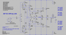
Check this out, my implementation of EC OPS.
BJT version in LTSpice, MOSFET in IRL.
It requires
- steady, low impedance drive (buffered VAS)
- low impedance bias spreader
K71 - MOSFET POWER BUFFER with ERROR CORRECTION - Google Photos

BJT version in LTSpice, MOSFET in IRL.
It requires
- steady, low impedance drive (buffered VAS)
- low impedance bias spreader
K71 - MOSFET POWER BUFFER with ERROR CORRECTION - Google Photos
Attachments
What seems to be missing here is a review of our own Bob Cordell's error correction amp that achieved performance most of us can only dream of.
http://www.cordellaudio.com/papers/MOSFET_Power_Amp.pdf
Jan
http://www.cordellaudio.com/papers/MOSFET_Power_Amp.pdf
Jan
Or Tooru Kuroda's power amplifier design from last year with an OPA627 front end and 0.00032% THD+N.
https://toragi.cqpub.co.jp/Portals/0/support/2019/10_kit/kuroda_amp1回路図(トラ技用20191221).pdf
https://toragi.cqpub.co.jp/Portals/0/support/2019/10_kit/図2.png?11992211816231
ゼロディストーション・パワーアンプ
https://toragi.cqpub.co.jp/Portals/0/support/2019/10_kit/kuroda_amp1回路図(トラ技用20191221).pdf
https://toragi.cqpub.co.jp/Portals/0/support/2019/10_kit/図2.png?11992211816231
ゼロディストーション・パワーアンプ
What seems to be missing here is a review of our own Bob Cordell's error correction amp that achieved performance most of us can only dream of.
His build quite impressively fills in the blanks from the previous theory and shows excellent measured performance. One thing that I see in his book that I am not sure about is performance after the error corrector clips. The error corrector results in lower than the actual impedance, so it seems there would be distortion as the error correction goes away and the emitter resistor dominates (even if the current is high enough that the virtual emitter resistance is negligible). I would be interested to simulate LKA's model to see what the voltage headroom requirements are for the bias network style error corrector versus the series error corrector I had started with.
Check this out, my implementation of EC OPS.
I like your schematic, one thing that is attractive is that you spread the voltage out enough to use largish resistors to transmit the error signal, so that they dominate over the virtual emitter resistance and you don't appear to need to trim after assembly.
I have better numbers than Kuroda, Cordell, Benchmark
That is extremely impressive to build and groom a setup to measure to this level. Good work!
It appears possible in simulation to build an error corrector with extra-ordinarily low distortion if one uses an opamp. I even dithered the resistor tolerances, and the distortion is still very good. Here is a concept using a low voltage rail to rail opamp as the difference amplifier. I am still showing concepts with the error corrector in series with an existing output, rather than integrated into the bias network. The distortion is <-110dB for 10Vpk into 8Ohms (or 6.25WRMS).
Attachments


Last edited:
It may be somewhere else on the schematic, but what I don't see are the LTspice FFT & timestep parameters for high resolution FFT.
That may be limiting your measurement; the amp may be better than what the FFT shows.
An example:
.param freq=1000
;param FFT=2**19 dlycyc=3 numcyc=2 ; set to 0.5M points
;param simtime=numcyc/freq+dlytime
;param dlytime=dlycyc/freq
;param timestep=(simtime-dlytime)/FFT
Jan
That may be limiting your measurement; the amp may be better than what the FFT shows.
An example:
.param freq=1000
;param FFT=2**19 dlycyc=3 numcyc=2 ; set to 0.5M points
;param simtime=numcyc/freq+dlytime
;param dlytime=dlycyc/freq
;param timestep=(simtime-dlytime)/FFT
Jan
Jan,It may be somewhere else on the schematic, but what I don't see are the LTspice FFT & timestep parameters for high resolution FFT.
That may be limiting your measurement; the amp may be better than what the FFT shows.
An example:
.param freq=1000
;param FFT=2**19 dlycyc=3 numcyc=2 ; set to 0.5M points
;param simtime=numcyc/freq+dlytime
;param dlytime=dlycyc/freq
;param timestep=(simtime-dlytime)/FFT
Jan
What exactly are you trying to achieve with all those statements.
Simply using:
.options plotwinsize=0
.options numdgt=12
Is all you need to get the most accurate high resolution FFT image IMO.
But you are right that since these instructions are missing, the image does not present the most accurate result.
Hans
Hans, those equations are meant to obtain max FFT resolution and lowest noise floor. They make sure that the FFT is synchronous with the signal, so that there is no spectral leakage without a window. Also the time step is set so that it is the exact value required by the synchronous FFT. The FFT value defined (like 10^19) gives also the value to set the FFT length to in the View|FFT window.
This is independent from numdgt and waveform compression. It is very similar to what you would do in ARTA or REW for max resolution, synchronous FFT.
The numcyc, numdly etc are not required for the FFT but set the simulation length and data collection length based on frequency for a nice 3-cycle display.
Jan
- Home
- Amplifiers
- Solid State
- Kolinummi concept for reducing crossover distortion implemented on Blameless