As a side note, using DC coupling is important when checking waveforms, especially when checking the gate drive for the power supply (not applicable here but would be if you were troubleshooting the power supply drive circuit).
That's the option on my scope in the 'CH'(annel) setting that says Coulping, yeah? I didn't even think to change that. It has been on AC this whole time. As for the BP1200 you posted a picture of, that's funny. I actually run one of those in my second car myself. Good little amp for what it is.
#17:
What were you using for ground?
I was using the center tap indicated, is that the correct thing to use? Sorry for so many posts, I didn't even catch yours in the process of posting pictures.
In some instances where DC needs to be ignored, AC coupling is OK but I leave my scope on DC coupling most of the time.
The secondary center tap is good for all waveforms/testing on the audio side of the transformer.
The secondary center tap is good for all waveforms/testing on the audio side of the transformer.
I should have caught this earlier,and the reason why I mentioned using the center tap as reference because this amp has a bridged output, which means the neg speaker terminal is not connected to the center taps.
I will study the photos later tonight and post any observation. This may take some back and forth, and the number of posts can't be helped,especially when dealing with this beast!
Sent from my HTC Desire 626 using Tapatalk
I will study the photos later tonight and post any observation. This may take some back and forth, and the number of posts can't be helped,especially when dealing with this beast!
Sent from my HTC Desire 626 using Tapatalk
Recheck the waveform on the LM361 using the secondary center tap and post screenshots.
You will find 4 U-shaped bars on either side of the board near each bank of outputs,8 in all.The bars carry the +/- rail voltages. With your DC voltmeter,measure the the rails with negative probe on the center tap post.
You might try removing the driver board on the bad output side and recheck the drive signal on the good side. I suspect the driver board may be bad.
Sent from my HTC Desire 626 using Tapatalk
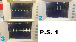
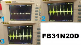
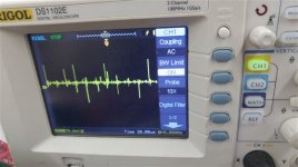
Hello again. Just updating that I will be following this advice tonight, to see what I get. However I did want to mention that those waveforms I posted of the LM361 are using the secondary center tap, same with the ones for the outputs posted after that.
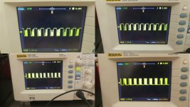
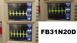
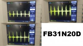
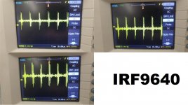
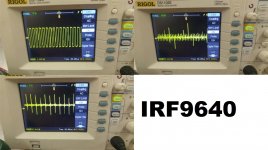
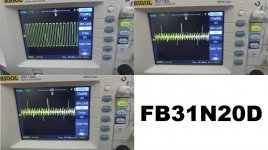
Okay, so I did a bit more testing as recommended. For the following tests, both driver boards have been removed from the amp, and the preamp/tone board is also removed from the amp. The amplifier has none of the FB31N20D FETs in it, but the IRF9640's are still installed.
I checked the voltage on the u-shaped bars, and I got ~58.0v and ~ -58.0v on the bars near the 9640 and FB31, respectively. This had very little variance, ~0.1v at most. All banks matched. I used B- as ground reference.
The first set of waveforms is from the outputs. All waveforms matched nearly identically (or at least identically enough I could not distinguish a difference) between banks. The first 3 are the 9640, second are the FB31'S. The secondary center tap is used as ground reference here.
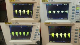
The next waveforms are from the power supply. I did note that one side was different than the other on one of the legs. B- is used as ground reference.
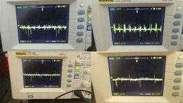
The last waveforms are of the LM361, pins 4, 9, and 11, respectively. The secondary center tap is used as ground reference here. I do apologize, as it appears I only have the waveforms of 4 & 9. I will try to grab 11 next time I have a moment to work on this, if it is needed.
I checked the voltage on the u-shaped bars, and I got ~58.0v and ~ -58.0v on the bars near the 9640 and FB31, respectively. This had very little variance, ~0.1v at most. All banks matched. I used B- as ground reference.
The first set of waveforms is from the outputs. All waveforms matched nearly identically (or at least identically enough I could not distinguish a difference) between banks. The first 3 are the 9640, second are the FB31'S. The secondary center tap is used as ground reference here.
The next waveforms are from the power supply. I did note that one side was different than the other on one of the legs. B- is used as ground reference.
The last waveforms are of the LM361, pins 4, 9, and 11, respectively. The secondary center tap is used as ground reference here. I do apologize, as it appears I only have the waveforms of 4 & 9. I will try to grab 11 next time I have a moment to work on this, if it is needed.
Attachments

Try one driver board at a time. If you happen to know which driver board was on the good side, use it. If not try one and then the other. Whichever driver board works best then move it to the other side. I suspect that the driver board on the "bad side" is the issue. Once you have determined if this is the case we can take the next step.
Sent from my HTC Desire 626 using Tapatalk
Sent from my HTC Desire 626 using Tapatalk
OK, I will try that tonight. How should I try it? Just install it and check the waveforms? I don't have enough FB31 to put them in (have 3/12 left), as long as it's OK to keep them out I'll do that.
You can remove all of the outputs FB31's and 9640's included.This will allow you to check waveforms and determine which driver board is bad. Did you say you have another 2500.1? If so you may be able to substitute the driver board's. Post pics of any driver boards you have,there were some revs made and you don't won't to mix and match.
Sent from my HTC Desire 626 using Tapatalk
Sent from my HTC Desire 626 using Tapatalk
![1002160418[1].jpg](/community/data/attachments/534/534493-3ee30c7431fc31ee89a22dc27855486e.jpg?hash=PuMMdDH8Me)
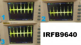
I have come bearing waveforms! All output transistors have been removed. I am using secondary center tap as ground. Driver boards have been labeled 1, 2, 3, and 4, to keep track. 1&2 are original, 3&4 are spares.
In the following waveforms, I have board 1 in the 'Good Side', labeled by me as banks 3 & 4. Both sets of waveforms were matching between banks.
In the following waveforms, I have board 1 in the 'Good Side', labeled by me as banks 3 & 4. Both sets of waveforms were matching between banks.
Attachments
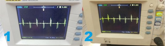
Did I miss something? Was the issue of the drive from the LM361 resolved? The following is approximately what you should have. Right-click to zoom in.
http://www.bcae1.com/temp/genericclassd1kicker550pt3b52idwaveforms.swf
http://www.bcae1.com/temp/genericclassd1kicker550pt3b52idwaveforms.swf
Check the DC voltages around the LM361 and the MC14060 which is right beside the 361 and post. Comparing the pictures you posted in #17 and #27 it appears you may have
A) Damaged the MC14060 and possible the LM361 or
B) The regulated +/-15 volt supply
A) Damaged the MC14060 and possible the LM361 or
B) The regulated +/-15 volt supply
PapaZBill, you were correct. I swapped the LM361, and got no new results. I did not remove the donor LM361, and then swapped the MC14060 (labelled CD04060DE on my amplifier), and now I have waveforms that look clean and exactly like what Perry's link shows. No messy waveforms whatsoever as were previously observed on 4/9/11. I will install driver boards tomorrow, and re-post the waveforms from the outputs, and see if you think it might be safe to install FETs again. Do you by chance have any resources on what the waveforms on the output should look like with the driver boards in? It doesn't have to be exact, just would like to know about what I might want to/expect to see. Thank you again for all of your help, I greatly appreciate all the advice and explanations you've given thus far.
Last edited:
Basically,what you see at pin 9 & 11 of the LM361 is what you should see at the gates of the output mosfets,present or not.
Sent from my HTC Desire 626 using Tapatalk
Sent from my HTC Desire 626 using Tapatalk
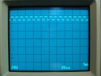
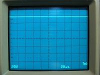
The attached photos show the drive signal and rail voltage. Your rail voltage will be different but you can see how the drive signal drives up and down from the respective rails and shows the amplitude of the drive signal.
Attachments

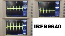
Okay, I popped the driver boards in. I now get this for the IRF and FB31. Note that the last two unlabeled waveforms are from bank 2, pin 2 of both IRF and FB; they were the only discrepancy between banks as far as waveforms go, the other three banks matched the corresponding waveforms almost identically. I believe this is the channel that was previously damaging FB31's, just to note.
Attachments

Without FETs in the circuit, the gate drive is the only waveform that you will have. When your scope is at 50mv/div, you're just looking at noise. The drain is at 0v and the source is at rail voltage. You cannot have any significant signal (only noise) on the drains without the FETs.
- Status
- Not open for further replies.
- Home
- General Interest
- Car Audio
- Kicker 2500.1 Protect Mode Issues [Repair]