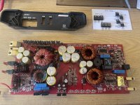
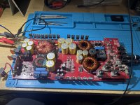
Kicker “Redline” 06 ZX750.1
All power supply mosfets literally exploded. Shielding on top inductor compromised, shielding on bottom inductor starting to flake off as well but not nearly as bad so I rewrapped both cores with 14AWG high-temp 200’c magnet wire, similar # of wraps @ 55 each, 30 on 1st layer, 25 on 2nd layer, to get near spec 135mH rating, ended up near 140mH (side note, idle current draw went from .7XXa to 1.1a after inductors rewrapped and reinstalled, I also replaced all power supply mosfets, a gate resistor on PS side and Output side, bi-polar transistors @ Q03, Q05, Q11, and Q103 and rewrapped inductors. Amp powers on out of protect and idles at 12v/1.1a with no output FETs installed.
Power Supply Mosfets
Gate: +4.25v
Drain: +12v & Square wave
Source: ~
Rectifier In
Cathode: square wave
Anode: +59v
Gate: square Wave
Rectifier Out
Cathode: square wave
Anode: -59v
Gate: square wave
High Voltage Regulator
Gate: +19v
Source: ~
Drain: +12v
Low Voltage Regulator
Gate: ~
Source: -19v
Drain: -12v
Hi Output mosfets (No FETs in board)
Gate: +50v
Drain: ~
Source: +59v
Low Side Output Mosfets (No FETs in board)
Gate: -59v
Drain: ~
Source: -59v
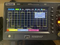
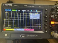
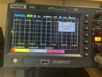
Updated values as of 3/18/21 with DMM checking square waves with Oscope. Perfect square waves up to LM361N before a slip on a voltage regulator caused a very audible fizzle somewhere and now squarewaves on lm361n are gone and 10 Ω resistor @ R260 looks to have a hole and measures 17ohm. Both removed and waiting on replacements.
Thank you for any and all help Perry 🖖🏼
All power supply mosfets literally exploded. Shielding on top inductor compromised, shielding on bottom inductor starting to flake off as well but not nearly as bad so I rewrapped both cores with 14AWG high-temp 200’c magnet wire, similar # of wraps @ 55 each, 30 on 1st layer, 25 on 2nd layer, to get near spec 135mH rating, ended up near 140mH (side note, idle current draw went from .7XXa to 1.1a after inductors rewrapped and reinstalled, I also replaced all power supply mosfets, a gate resistor on PS side and Output side, bi-polar transistors @ Q03, Q05, Q11, and Q103 and rewrapped inductors. Amp powers on out of protect and idles at 12v/1.1a with no output FETs installed.
Power Supply Mosfets
Gate: +4.25v
Drain: +12v & Square wave
Source: ~
Rectifier In
Cathode: square wave
Anode: +59v
Gate: square Wave
Rectifier Out
Cathode: square wave
Anode: -59v
Gate: square wave
High Voltage Regulator
Gate: +19v
Source: ~
Drain: +12v
Low Voltage Regulator
Gate: ~
Source: -19v
Drain: -12v
Hi Output mosfets (No FETs in board)
Gate: +50v
Drain: ~
Source: +59v
Low Side Output Mosfets (No FETs in board)
Gate: -59v
Drain: ~
Source: -59v
Updated values as of 3/18/21 with DMM checking square waves with Oscope. Perfect square waves up to LM361N before a slip on a voltage regulator caused a very audible fizzle somewhere and now squarewaves on lm361n are gone and 10 Ω resistor @ R260 looks to have a hole and measures 17ohm. Both removed and waiting on replacements.
Thank you for any and all help Perry 🖖🏼
Attachments
Last edited:
I'm not going to try to cover all of this in one post.
What scope make/model?
The terminal names of the PS FETS are wrong.
The rectifiers should not have DC on their outer legs. What's the DC voltage between the negative speaker terminal and the primary ground?
The rectifier terminal names are wrong.
What scope make/model?
The terminal names of the PS FETS are wrong.
The rectifiers should not have DC on their outer legs. What's the DC voltage between the negative speaker terminal and the primary ground?
The rectifier terminal names are wrong.

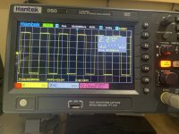
Oscilloscope: Hantek DSO2D15 (with further digging, learning, testing I found I had some settings wrong and calibration seems to be quite good, it’s only .5v off at most)
PS Fet terminal names corrected and noted, ty
Retested rectifiers and they are barely getting between .4-.8mv on outter legs, which I’m sure is just feedback
Primary ground to Negative speaker terminal: 4mv
Rectifier terminal names are corrected and noted, ty again.
And ya I know it’s a lot, my bad, just trying to give all info I think might be pertinent. Also I’m pretty sure I had a square wave on my voltage regulators before I slipped between legs 2&3 on right v.reg and heard a spark 1/2 second later but didn’t see where it came from (first and last time I don’t completely concentrate on probing and making more problems ...) which I’m sure just introduced more problems ...think I found output drive ic, CD4060BM, which has triangle/square waves, going to reprobe and retest with correct settings and new DVM instead of cheap DVM. What would prevent V.Reg from getting a square wave? And after that I need to figure out why output is not getting square waves, off to read research and learn, ty in advance.
Attachments
Last edited:
With no power applied, connect your ohm meter between the B+ terminal and the negative speaker terminal. Note the reading. Then twist/push/pull on the power transformer. Does that make the readings on the meter change?
Also measure the resistance between the negative speaker terminal and the primary ground.
Please break up the text more to make the multiple topics easier to see.
The voltage regulator should not have a square wave on it.
There's no driver IC in this amp like some other amps. This amp and others like it make the drive circuit from groups of other components. The basic circuit can be found in the attached diagram.
Attachments
B+ terminal & Negative speaker terminal @ 6kOhms and climbing past 60kOhms with no manipulation of transformer, twisting and pulling had no effect on steady climb of reading.
Primary ground & Negative speaker terminal @ 9.9kOhms, no fluctuation
Will do, I’ll try to break up each symptom/etc into its own section
Thank you for the service manual and heads up on drive output for this type of amp, I have it saved in my main amp repair repository. I’m not proficient at reading amp schematics as of yet but studying, I’m sure the answer is right in front of my face once I know how to properly decode everything 🙂
ty Perry
Do you have the repair tutorial?
If so, the manual was in the JBL folder.
With the readings I asked you to take, I was looking for a reason that you had a square wave on the regulators but I don't see one.
From this point on, use the negative speaker terminal as the reference (black probe) for any voltage readings in the audio circuit, unless otherwise specified.
What's the DC voltage from the gate to source (black probe) for the low-side FETs?
The names for the FET terminals are wrong for the outputs as well. Look up the datasheets for the FETs (or any component) to see the correct pin configuration.
Last edited:
I want to double/triple check all of my work with new quality DMM and scope with proper settings, using negative speaker terminal as main ground, before going forward, I don’t trust some of my work or that cheap o DMM I 1st used.
I’ll take that reading as well while double/triple checking.
I’ll also correct those terminal names and make sure to check data sheet from now on, I want to know each type. Ty.
I’ll take that reading as well while double/triple checking.
I’ll also correct those terminal names and make sure to check data sheet from now on, I want to know each type. Ty.
Confirming R260 is marked 100? which I know is a 10Ω, it’s reading as 17Ω, almost double 🥴 going through everything again now with a microscope eye lol, LM361N is bad as well, parts incoming!
Edit: I just realized it could also read 180, with is 18 Ω and within spec @ 17 Ω. Ya def need to confirm when someone can, ty
Edit: I just realized it could also read 180, with is 18 Ω and within spec @ 17 Ω. Ya def need to confirm when someone can, ty
Attachments
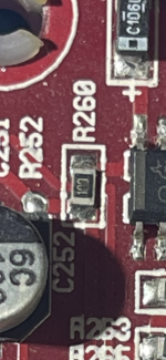
It's marked 100. 10 ohms. Doesn't that feed the 4060 and C260?
Why do you believe that the LM361 is defective?
Why do you believe that the LM361 is defective?
Last edited:
Yessir it does.
I was getting square waves on the out pins of the LM361n ...before I slipped while probing a voltage regulator ...about a second later after slipping I heard a spark/fizzle in the area (but did not see it. Now I get no square waves from it :/ but then again maybe it was that 10 Ω resistor that blew? Reprobing everything cuz I’m looking at some of my above readings and some make no sense :/
I was getting square waves on the out pins of the LM361n ...before I slipped while probing a voltage regulator ...about a second later after slipping I heard a spark/fizzle in the area (but did not see it. Now I get no square waves from it :/ but then again maybe it was that 10 Ω resistor that blew? Reprobing everything cuz I’m looking at some of my above readings and some make no sense :/
Answer to last question asked in February,
Gate to Source (black probe on source/3rd leg) DC voltage reading 0.1mv on DMM
Gate to Source (black probe on source/3rd leg) DC voltage reading 0.1mv on DMM
The 4060 may be defective. That's the source of the square wave for the class D section.
R260 feeds the 4060 and C260. What'e the resistance across R260?
When you refer to an old post, quote it and then answer it.
R260 feeds the 4060 and C260. What'e the resistance across R260?
When you refer to an old post, quote it and then answer it.
I removed R260 to test out of circuit (just in case, still learning what I can test in/out of circuit) and it’s reading 17ohms, which is almost double its rated 10ohm and far past the 10% threshold correct? And across empty pads of R260 read 42 MΩ.
Last time I probed the CD4060BM my notes say I was getting square waves at pins 1, 2 and 13, 14, 15. In going to reprobe now.
I do not have a replacement 10 Ω resistor yet for R260, it’s incoming along with an extra lm361n, which I removed from board as well.
And will do, I will also try to not to flip flop across so many boards, I feel like I’m doing that too much, no real direction i apologize.
im going to reconfirm power supply section is properly working after that slip, reprobing and with DMM as well to double check.
10% tolerance is rare. That's likely a 5% tolerance. It's well out of tolerance.
Pin 5 (80kHz) of the 4060 is the one that is used by the class D section.
Pin 5 (80kHz) of the 4060 is the one that is used by the class D section.
See also post 14.
If you're taking notes, I'd suggest making a template something like the one below to keep in your notes. Save it with the photos you take of the board and components.
If you're taking notes, I'd suggest making a template something like the one below to keep in your notes. Save it with the photos you take of the board and components.
I used your template to make this .pdf. The .zip file is an excel file of the template.Didn't attach.
Attachments
Thanks for posting. Post any other notes like those in posts 15-17 in the following thread to minimize contamination of a repair thread.
https://www.diyaudio.com/community/threads/taking-notes-and-photos.384345/post-6973639
https://www.diyaudio.com/community/threads/taking-notes-and-photos.384345/post-6973639
Last edited:
O wow ok, ty so much fellas, this board seems like it’s gona be a doozy cuz so many pieces in so many “random” areas were blown so this helps a lot, especially since I am so new to the field/hobby.
I’ll report back once replacements get in and i take proper readings, complete notes, etc.
Ty 🙂
I’ll report back once replacements get in and i take proper readings, complete notes, etc.
Ty 🙂
So after about 4 more hours of work installing new parts, reseating a few others, etc I got this bad boy up and running, waves look super clean on both sides for both banks, idles nice and cool and sounds great as well.
Thank you for all your help Perry, I’m really starting to feel like I’m understanding more and actually having great results to match. My bench looks like I’m taking online courses with all the notes & diagrams lol. Hoping to score a video card soon too so I can get my PC up&running, getting anxious on diving into your guide, Ty bro 🙂
Thank you for all your help Perry, I’m really starting to feel like I’m understanding more and actually having great results to match. My bench looks like I’m taking online courses with all the notes & diagrams lol. Hoping to score a video card soon too so I can get my PC up&running, getting anxious on diving into your guide, Ty bro 🙂
Attachments
-
 001D435B-FDA2-4FB0-8B01-5F039CBF556A.jpeg569.7 KB · Views: 80
 -
 B5FBEA5B-69BE-4E32-B470-711F75D4D6E8.jpeg453.6 KB · Views: 60
 -
 BC999471-58BA-40EA-A2D3-95F8AC909732.jpeg449.9 KB · Views: 54
 -
 3C09ABEB-9874-471A-8BEF-9ADDE818C7B3.jpeg476.1 KB · Views: 58
 -
 2A14DA85-BB01-49C4-B710-B42B0DBFBFA7.jpeg474.4 KB · Views: 60
- Home
- General Interest
- Car Audio
- Kicker 06 ZX750.1